The behavior of copper (Cu) diffusion at different storage temperatures of heavily boron-doped silicon substrates is investigated. The surface Cu concentration of the substrate with quantitative Cu contamination exhibits an initial increase followed by a subsequent decrease upon storage at 25 °C and 85 °C. The surface Cu, originating from the out-diffusion, can be effectively removed through RCA cleaning. The polysilicon film, prepared by low-pressure chemical vapor deposition (LPCVD) on the back of the substrate, exhibits a pronounced inhibitory effect on the out-diffusion of Cu. This phenomenon can be attributed to the effective gettering of Cu by both grain boundaries and disordered grain structures within the polycrystalline silicon film. Additionally, the multilayered structure of the polysilicon film exhibits enhanced gettering capabilities. The enhanced gettering effectiveness achieved by the multilayer polysilicon film can be attributed to an increased number of interfaces between layers.
1. Introduction
With the development of the microelectronics industry, the ultra-large-scale integrated circuits (ULSI) requirements for silicon materials are increasing. Currently, p+ silicon substrates doped with highly concentrated boron serve as epitaxial substrates and play a critical role in the fabrication of advanced integrated circuits such as microprocessors, highvalue logic devices, and insulated gate bipolar transistors (IGBTs).The utilization of p+ epitaxy for complementary metaloxide semiconductor logic devices can effectively mitigate noise in both analog and digital circuits. However, transitional metallic contamination in p+ silicon substrates severely degrades the electrical properties of substrates, and further causes the device failure. On the one hand, metal impurities cannot be completely avoided, due to the purity of the initial material, and the subsequent processing steps.5 On the other hand, the increasing performance of electronic devices also places stringent requriements on the concentration of metal contamination. Metallic contamination is specied less than 1010 atom per cm2 in advanced ULSI technologies. However, contamination up to 1012 atom per cm2 has been observed during processing.6 Among all the metallic contaminants, copper (Cu) is recognized to be the most problematic one. Cu is not only easily transferred to substrates from optimized process tools and low-quality gases and chemicals, but also greatly reduces the yield of silicon devices.Contamination of Cu can degrade the dielectric properties of gate oxides causing premature breakdown and diffusion into the bulk of the silicon material resulting in an increase of the junction leakage and a reduction of the minority carrier lifetime.
Various studies have been conducted on gettering techniques to remove metal impurities from the active region of devices. Gettering techniques using oxide precipitates, polysilicon back seal, ion implantation, and shallow dopants in silicon have been developed over the past few decades. In particular, polysilicon gettering, as an out gettering method, can form the metal precipitates to removal the metal impurities. The method can effectively inhibit the diffusion of contaminated metals and enhance its gettering effectiveness,which is resulted from the grain boundaries and highly disordered lattice structure.The polysilicon lms can be obtained by a variety of chemical vapor deposition techniques, including low pressure (LPCVD), atmospheric pressure (APCVD), and plasma enhanced (PECVD). LPCVD, as it affords high deposition volumes, has been studied over the past few decades for numerous electronic applications. However, there exists a signicant disadvantage of warpage increase during LPCVD which affects the subsequent epitaxial growth and chemical mechanical polishing. The warpage increase of the silicon substrates is caused by the residual stress within the polysilicon lm.The removal of residual stresses of polysilicon lm is essential, in order to achieve optimum device performance.
2. Experimental
2.1 Substrates
The heavily boron-doped silicon substrates used in this study are adjacent, as-sawn, sister substrates taken from a highperformance monocrystalline silicon ingot. The concentration of bulk Cu is less than 5.0 × 10¹² atoms per cm3 . The monocrystalline silicon substrates were processed according to the standard process of cutting, grinding, acid etching, back treatment, polishing, and post-polish cleaning procedures. The thickness of heavily boron-doped silicon substrate is 625 mm aer all the treatment. For cleaning, all the substrates were thoroughly rinsed through RCA cleaning processes to remove surface metals from the substrate as much as possible.
2.2 Pre-treatment of Cu contamination
In order to investigate the effect on Cu diffusion, the p+ substrates were pretreated for Cu contamination according to the reported literature.18 Briey, CZ, a p-type substrate with a diameter of 150 mm, with medium oxygen content was chosen. The substrate has a h111i crystal plane and a resistance of 0.002 U cm. The CZ substrates were contaminated from CuCl2 standard solution. The resulting surface contamination was in the range of 5.0 × 10⁹ to 5.0 × 10¹³ atom per cm2 .
2.3 Effects of polysilicon film on Cu diffusion
Thicknesses and uniformity of polysilicon lms were measured by an optical thickness instrument (F50 Filmetrics) which utilizes a five-point test method. The geometric parameters were measured by a substrates surface atness measuring instrument (ADE 7200). The microstructures were determined using ultrahigh resolution field emission scanning electron microscope (SEM, Hitachi SU8000) and atomic force microscope (AFM). The precipitation of these metals on the substrate surface was monitored by inductively coupled plasma mass spectrometry (ICP-MS, Agilent 7900). HNO3 (69%), HF (49%) and H2O2 (31%) were used for sample pretreatment as well as for the preparation of the blank and standard solutions for ICP-MS analysis.
3. Results and discussion
3.1 Out-diffusion of Cu in p+ substrates
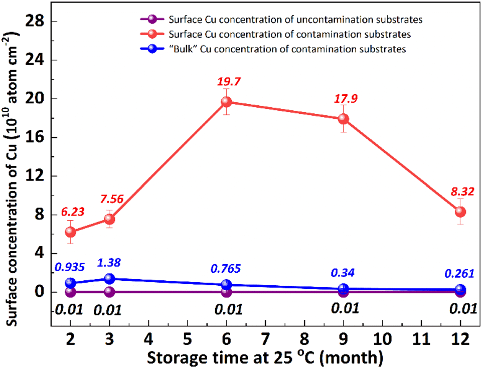
It is well known that the out-diffusion of Cu in silicon is affected by temperature, doping type, doping concentration, and silicon lattice integrity.Fig. 1 shows the Cu concentration on the front surfaces of substrates after the storage at room temperature (25 °C) for 2, 3, 6, 9, 12 months. All the substrates were cleaned by RCA cleaning before being placed at room temperature to ensure that the surface Cu concentration was below 0.02 × 10¹⁰ atoms per cm2 . However, the Cu concentration after thermal treatment at 300 °C for 2 h increased to about 20.0 × 10¹⁰ atoms per cm2 , indicating that the Cu contaminated on the surface diffused into the bulk.In the contaminated substrates, the concentration of surface Cu first increased, then decreased, reaching its maximum after 6 months. This increase in the front surface Cu concentration by 2–3 orders of magnitude indicated that bulk Cu out-diffusion occurred during the room temperature storage. By contrast, there was no significant increase in surface Cu concentration for uncontaminated substrates. This is since the out-diffusion rate is greater than the in-diffusion rate in the early stage, while the opposite trend in the later stage. Then the surface of the same substrate was cleaned by RCA cleaning, and the Cu concentration on the surface after thermal treatment at 300 °C for 2 h was examined as shown in Fig. 1 by the blue symbol, which represents the concentration of bulk Cu. The observed concentration is significantly lower than the initial bulk Cu concentration, indicating that there is a diffusion of Cu from the bulk towards the surface.

Fig. 1 Variations in Cu concentration on p+ substrate front surfaces after storage at 25 °C for different periods of time. The “contaminated substrates” represents the substrates treated by CuCl2 for 30 min. The “bulk Cu concentration” represents the surface Cu concentration of substrate after by RCA cleaning and thermal treatment at 300 °C for 2 h.
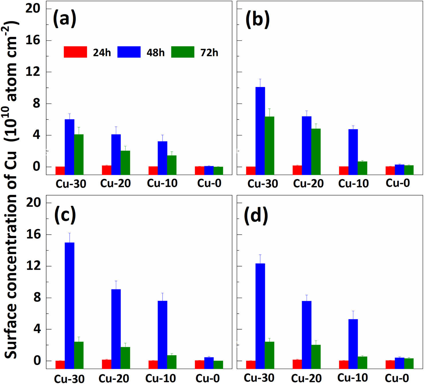
The impact of re-cleaning on surface Cu concentration of p+ substrates with thermal treatment is depicted in Fig. 3. After the initial 85 °C thermal treatment (as shown in Fig. 2), the surface Cu concentration increases. Subsequently, following the application of the RCA cleaning method (depicted by red column), the surface Cu concentration returns to its initial level, remaining below 0.02 × 10¹⁰ atoms per cm2 . However, there is a subsequent increase in the surface Cu concentration after the second thermal treatment at 85 °C for 48 h (illustrated by blue column), albeit at a value lower than that observed after the firrst thermal treatment. The substrate subjected to an initial heat treatment of 48 hours exhibits the lowest concentration of Cu on its front surface during the subsequent heat treatment. The findings suggest that a significant amount of Cu out-diffusion and thorough RCA cleaning can effectively eliminate the bulk Cu contamination. In other words, Cu out-diffusion can be described as “limited source diffusion”, and the contaminated Cu in the bulk can be effectively eliminated by accelerating its out-diffusion followed by thorough RCA cleaning. It also suggests that the outer diffusion to the surface is not in the form of copper–silicon compounds, but may instead form relatively weak chemical bonds with surrounding atoms.

Fig. 3 Effect of re-cleaning on surface Cu concentration of p+ substrates with different thermal treatment times. The (a), (b), (c) and (d) correspond to the “first thermal treatment” time of 12, 24, 48 and 72 hours respectively. The 24 h, 48 h and 72 h in (a) represent the time of the “second thermal treatment”, respectively. The Cu-30, Cu-20, Cu-10, and Cu-0 represent the substrates with different amounts of contamination in Fig. 2 respectively.
3.2 Effect of backside polysilicon film on Cu out-diffusion
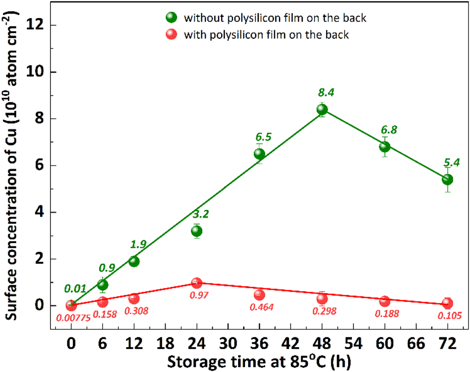
Impurity gettering in silicon is an indispensable technology to avoid device degradation by heavy metal contamination.Polysilicon back seal, which refers to the deposition of thin polysilicon films on the back side of silicon substrates, is a commonly used out gettering technique. The previous studies have demonstrated that the implementation of a polysilicon film at the backside of p+ substrates effectively inhibits the diffusion of segregated metal from the bulk silicon to the epitaxial layer.This is attributed to the extremely low diffusivity of metal in polysilicon, making it an exceptional getter material.The impact of polysilicon film growth on the backside of the substrate on Cu out-diffusion at 85 °C was investigated, as shown in Fig. 9. The p+ silicon substrates were subjected to a 20 minutes contamination process with CuCl2 and subsequently cleaned using RCA cleaning to ensure that the surface Cu concentration is below 0.02 × 10¹⁰ atom per cm2 . After undergoing thermal treatment at 85 °C for 48 hours, the p+ substrates without a polysilicon film exhibit a surface Cu concentration of 8.4 × 10¹⁰ atom per cm2 , indicating the bulk Cu out-diffusion to the front surface of p+ substrates. The Cu concentration on the front surface of the p+ substrate, with a polysilicon film grown on the back, exhibits an initial increase followed by a subsequent decrease, reaching a maximum value of 0.97 atom per cm2 after 24 hours of thermal treatment at 85 °C. The obtained result suggests that the presence of a polysilicon film on the backside of the substrate effectively inhibited bulk Cu out diffusion to front surface.

Fig. 9
4. Conclusion
The surface Cu concentration of the p+ monosilicon substrate, which has been quantitatively contaminated, exhibits an initial increase followed by a subsequent decrease with the increase of storage time. It is noteworthy that the highest surface Cu concentration is observed after 6 months of storage at 25 °C, while a similar peak is reached after 48 hours of storage at 85 ° C. The bulk Cu can undergo diffusion on the substrate surface through out-diffusion for a duration of 48 hours at a temperature of 85 °C, while surface Cu can be effectively eliminated by RCA cleaning. Consequently, the repeated application of both out-diffusion and RCA cleaning processes enables efficient elimination of bulk Cu contamination. The out-diffusion of Cu can be effectively prevented by the growth of a polysilicon film on the back of the substrate, due to enhanced Cu precipitation facilitated by grain boundaries and disordered structure within the polysilicon film. Moreover, increasing temperature and reducing grain size can eliminated internal residual stress in LPCVD-deposited polysilicon films.
上一篇: 电化学方法实现的纳米多孔硅材料及其应用