Abstract
Elucidating the complex interactions between the work material and abrasives during grinding of gallium nitride (GaN) single crystals is an active and challenging research area. In this study, molecular dynamics simulations were performed on double-grits interacted grinding of GaN crystals; and the grinding force, coefficient of friction, stress distribution, plastic damage behaviors, and abrasive damage were systematically investigated. The results demonstrated that the interacted distance in both radial and transverse directions achieved better grinding quality than that in only one direction. The grinding force, grinding induced stress, subsurface damage depth, and abrasive wear increase as the transverse interacted distance increases. However, there was no clear correlation between the interaction distance and the number of atoms in the phase transition and dislocation length. Appropriate interacted distances between abrasives can decrease grinding force, coefficient of friction, grinding induced stress, subsurface damage depth, and abrasive wear during the grinding process. The results of grinding tests combined with cross-sectional transmission electron micrographs validated the simulated damage results, i.e. amorphous atoms, high-pressure phase transition, dislocations, stacking faults, and lattice distortions. The results of this study will deepen our understanding of damage accumulation and material removal resulting from coupling between abrasives during grinding and can be used to develop a feasible approach to the wheel design of ordered abrasives.
1. Introduction
The gallium nitride (GaN) single crystal is the semiconductor with the highest application potential for manufacturing chip wafers due to the large bandwidth, high breakdown voltage, high electron mobility, and stable chemical and physical properties under extreme conditions . To fabricate thin chip wafers, bulk GaN crystals must be processed using a sequence of machining methods, including wire saw cutting, grinding, lapping, and polishing. Large chip wafers cannot be machined by lapping and are mainly machined by wire saw cutting, self-rotating grinding, and polishing. Self-rotating grinding can achieve the highest material removal and accurately control the surface shape and thickness of wafers. Self-rotating grinding has thus become necessary for backthinning of chip wafers. However, brittle fractures or micro cracks induced during grinding process can severely deteriorate the application accuracy and service life of crystal components. Therefore, numerous researchers focused on conducting polishingand high-energy beam etching of GaN semiconductors to eliminate the brittle damages of components. Kubota and Iwakiricarried out a tribochemical reaction to polish GaN substrates, producing a smooth surface with a root-mean-square roughness of 0.133 nm. The tribochemical reaction produced an oxide layer on the substrate surface, enabling removal of the work material under low stress. Pan et al performed chemical–mechanical polishing (CMP) tests on GaN semiconductors in conjunction with the electro-Fenton process to promote material removal. Zhang et al polished GaN wafers using plasma and electrochemical etching. The wafer surface had subnanometer-scale roughness, and materials were removed at the atomic scale. Although plastic surface free of surface and subsurface cracks was achieved using CMP or high-energy beam etching technologies, the low material removal efficiency of polishing and etching has hindered the large-scale industrial production and application of GaN chips.
The material removal efficiency of grinding is 105–107 times that of polishing, and plastic removal produces a considerably lower surface roughness and damage depth than brittle removal. Ductile grinding of hard and brittle crystals could effectively improve the surface quality and reduce the subsurface damage depth, thereby reducing the time required for subsequent polishing. Therefore, considerable effort has been expended to achieve ductile grinding of hard and brittle crystals, to improve the processing efficiency by ensuring the surface integrity of the crystal components. Shamray et al investigated the ductile-to-brittle transition behaviors of Si3N4 ceramics, and a Si3N4 substrate with a ductile surface and subsurface was obtained by controlling the maximum undeformed chip thickness. Yang et al investigated the ductile removal phenomenon of 3C-SiC involved in precision grinding process. Electrolytic in-process dressing was found to facilitate the generation of a compressive residual stress, enabling ductile removal of 3C-SiC. Wang et al analyzed how the removal mode affected the acoustic emission (AE) and force during grinding of sapphire. The depth of the ductile-to-brittle transition region could be monitored using the AE data and force curves.
2. Simulation and experimental conditions
2.1. Simulation conditions
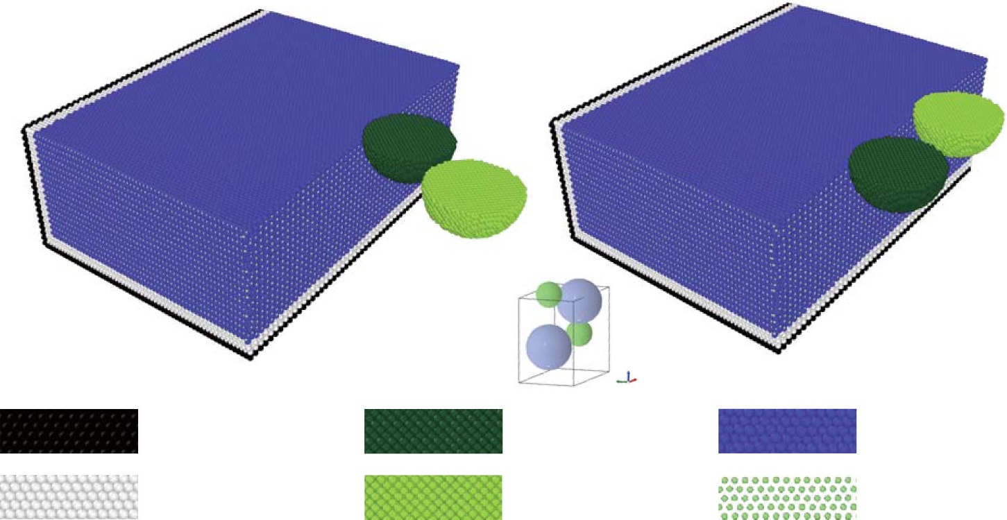
Two kinds of MD models for double-grits interacted grinding of GaN crystals were established using LAMMPS software. Both models consisted of a workpiece with a dimensions of 27.5 nm × 20 nm × 10 nm and two hemispherical abrasives with a radius of 3 nm. Three kinds of atoms were used in both the abrasive and workpiece models, namely, boundary, thermostat, and Newtonian atoms. The atomic positions in the boundary layer were fixed to prevent the workpiece from translating under the action of the grinding force. The coupling constant of the thermostat was selected to be 0.1 ps. The interacted distance of the two abrasives perpendicular to the grinding direction is called the transverse interacted distance, La. The interacted distance of the two abrasives along the grinding direction is called the radial interacted distance, Lb. Figure 1(a) shows the first model in which both La and Lb (=6 nm) are nonzero. Figure 1(b) shows the second model, in which only La is nonzero. All the grinding simulations were performed on the (0001) plane and along the direction. The grinding depth, grinding length and speed were set as 2 nm, 17 nm, and 50 m·s −1 , respectively. The relaxation and grinding processes of the abrasives and work material were simulated in the NVT and NVE ensembles, respectively. The two abrasives cut the workpiece simultaneously during the simulation.

Fig1
2.2 Experimental conditions
To validate the simulated results, an grinding experiment was performed on monocrystalline GaN using a ultraprecision selfrotating grinder, as shown in figure 2. The GaN specimen was 10.5 mm long, 10 mm wide, and 0.35 mm thick. To ensure that the GaN specimen was not damaged during preparation for the grinding test, CMP was performed on the specimen to achieve a surface roughness below 2.0 nm in Ra. Ceramic bonded diamond grinding wheels with mesh size of #8000 and diamater of 125 mm were used in the grinding experiment. The rotational speeds of the wheel and workpiece were 1500 and 100 r·min−1 , respectively. The feed rate was 12 µm·min−1 . Oil coolants were used in grinding process to decrease the grinding temperature and wheel wear. After the grinding test, an TEM sample of the ground subsurface was prepared by using a focused ion beam, and the subsurface damage was analyzed by the crosssectional TEM method. The accelerating voltage, TEM linear resolution, high-resolution TEM (HR-TEM), TEM magnification, and scanning transmission electron microscopy (STEM) magnification of the TEM (Talos F200x, USA) are 200 kV, 0.14 nm, 0.1 nm, 25–1500 000, and 150–2300 000, respectively.
3. Results and discussions
3.1. Grinding force and coefficient of friction
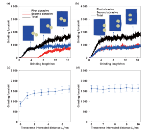
Grinding force is an important index for evaluating the machining effect during the grinding process, and indirectly reflects the material removal process and interaction between the abrasives and workpiece. Figure 3 shows the grinding forces under different interacted conditions. Both figures 3(a) and (b) indicate that as the grinding length increases, the grinding force increases and then stabilizes. Therefore, the average grinding force at the stable grinding stage can be used to analyze the influence of the interacted distance on the grinding force. Figure 3(a) also shows that the grinding force is smaller for the second abrasive than the first abrasive because of the elimination of coupling actions between the two abrasives. Figure 3(c) shows that for Lb = 6 nm and increasing La, the grinding force increases and then stabilizes. This result is obtained because increasing La weakens the coupling between the two abrasives, increasing the contact area between the workpiece and abrasives. Figure 3(d) shows that for noninterfering abrasives, there is a specific La at which there is no discernible coupling between the abrasives and the grinding force is approximately twice that of a single grit, that is, La has no discernible effect on the grinding force.

Fig3
3.2. Stress distribution
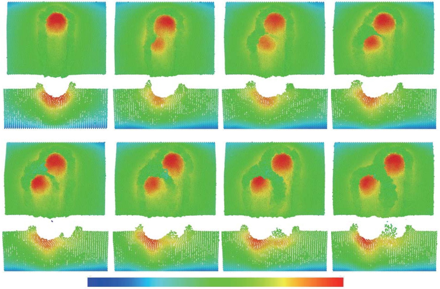
The stress investigated in this study corresponds to the von Mises stress, which was calculated by the spatial average method. Figure 5 presents the stress distributions for different transverse interacted distances when the radial interacted distance is 6 nm. The average stress induced by the second abrasive during double-grit grinding (~49.5–57.5 GPa) is smaller than that induced during single-grit grinding (~58.1 GPa) because of the elimination of the coupling to the first abrasive. When the transverse interacted distance is 1 nm, the average stress induced by the second abrasive is 14.8% lower than the average stress induced during single-grit grinding. As the transverse interacted distance increases, the coupling removal of the first abrasive weakens, causing the stress induced by the second abrasive to gradually increase and approach that induced during single-grit grinding.

Fig5
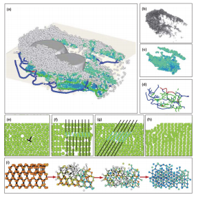
It is crucial that MD simulations accurately predict material damage phenomena. Therefore, it is particularly important to determine the subsurface damage mechanism of GaN crystals during interactive double-grit grinding. The machining scale in an MD simulation is considerably smaller than the depth of the brittle-to-ductile transition region in GaN crystals. Thus, the simulated subsurface damage is plastic damage, as shown in figure 7. The simulated results demonstrate that the plastic damage of GaN crystals induced by double-grits grinding is dominated by the amorphous transition, high-pressure phase transition, dislocations, stacking faults, and lattice distortions. The atoms in the chips and groove surfaces have high energy and weak structural stability and are therefore most prone to amorphization . The results of Zhang et al and Jiang et al lead to the conclusion that the maximum stress induced by machining does not occur at the ground surface underneath the abrasive but at a certain distance from the ground surface in the plastic zone. Therefore, the highpressure phase transition zone lies below the amorphous layer. The plastic zone is surrounded by a large number of stacking faults and dislocations because of the effect of subsurface stress at the boundary of the plastic zone . To eliminate the interference of elastic deformation on the identification of lattice distortion, we selected an area far away from the abrasive after elastic recovery to identify the lattice distortion. Therefore, the results presented in figure 7(h) were confirmed to be lattice distortion rather than elastic deformation. Figure 7(i) shows the phase transition path from hexagonal.

Fig7
4. Conclusions
The effect of coupling between abrasives on damage accumulation and material removal during grinding of GaN crystals was investigated by conducting MD simulations of interactive double-grit grinding of monocrystalline GaN. The simulated grinding force, coefficient of friction, stress distribution, plastic damage behavior, and abrasive damage were analyzed. The following conclusions were drawn from the study.
下一篇: 通过全夹层晶圆安装技术改进半导体芯片