ABSTRACT: Silicon wafers have been widely used in semiconductor manufacturing, and chipping issues often highlighted during wafer dicing which affects device performance and reliability. The phenomenon of chipping has been observed to have detrimental effects on die strength, leading to the potential of crack formation. Cracks became a major concern because its sometimes undetected during testing and had been reported to cause malfunctions at user applications. This study aims to comprehensively analyze the fragile behavior of silicon concerning its chipping and flexural strength performance, providing valuable insights for engineering applications. The research employed new wafer mounting techniques, including chipping analysis, a three-point bending test and scanning electron microscopy (SEM) to reduce silicon die chipping and increase the flexural strength by evaluating the novel semi and full sandwich wafer mounting techniques. The study demonstrated that the implementation of novel full sandwich mounting technique had improved significantly the silicon die chipping and flexural die performance among all the wafer mounting techniques.
1.INTRODUCTION
Silicon has been widely used in wafer fabrication in semiconductor manufacturing. The reason silicon is more popular for wafer fabrication is due to its abundant element on earth which ensures a stable supply for wafer fabrication. Technology and innovation in the semiconductor sector have been developing at an incredible rate in recent years and silicon wafers have become the backbone of the integrated circuit industry. Silicon is a material that belongs in the category of semiconductors because, under certain circumstances, it has the potential to conduct electricity. It is possible to alter its conductivity by a process known as doping, which involves the introduction of impurities. Additionally, silicon is preferable due to its higher melting point. Because of its high melting point, silicon has an additional advantage which can resist high temperatures during the fabrication process. This feature is critical in the manufacture of integrated circuits, where silicon wafers are subjected to extreme heat.
However due to silicon brittle nature , it has a tendency to chip or crack when subjected to mechanical stress or impact. It is a severe issue in silicon wafer manufacturing that may result in yield loss and lowering die strength performance. Chipping was the main concern in the wafer dicing process since it is unavoidable and could generate cracks during its application. Chipping is the term used to describe the area that is taken from the edge of the silicon die during the wafer sawing process as per “Fig. 1” below. The most concerning scenario was the crack generated by the chipping that sometimes can not be detected during testing and failed during application on the customer side.
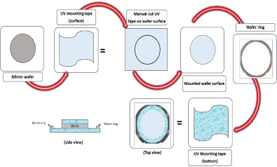
Since the wafer mounting process has the potential to improve the chipping performance, the new mounting techniques will be evaluated and compared with the conventional wafer mounting method. Conventional wafer mounting is a process whereby a wafer is attached to a wafer ring by a mounting tape which acts as a carrier for the wafer dicing process as described in “Fig. 2”. The conventional mounting technique has its own weakness whereby the wafer does not have enough support during the dicing process which may cause more vibration resulting in higher chipping results.

Fig. 2. Conventional wafer mounting technique.
During the wafer mounting process, both ultraviolet (UV) mounting tape and non-UV mounting tape were often utilized on the manufacturing floor. UV mounting tape, in comparison to non-UV mounting tape, has a stronger adhesion strength , which makes it possible to hold the back of the wafer firmly. The adhesive on the surface of wafer mounting tape secures the wafer's position during the wafer dicing procedure. The usage of high adhesive tape was done in order to reduce topside and backside chipping that occurred during the wafer dicing process. Bryan Christian claimed that the vibrations created by severe chipping during mechanical dicing can lead to cracks in the silicon die. This is why the UV tape was fixed for this activity in order to achieve the objectives of lower chipping and higher flexural strength performance. The assessment of novel semi and full-sandwich wafer mounting techniques was carried out, comparing both chipping and die strength performance against the conventional wafer mounting technique. The semi sandwich wafer mounting technique was designed to provide a cushioning effect during the wafer dicing process which may reduce the vibration and chipping as well. The semi sandwich wafer mounting technique process approach was by applying the wafer surface with additional mounting tape which has been described in “Fig. 3”. The wafer surface was laminated first by the mounting tape and then continued as per the normal wafer mounting process.

Fig. 3. Semi sandwich wafer mounting process.
2. MATERIAL AND METHODOLOGY
2.1. Wafer Back Grinding
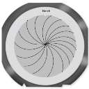
In this activity, 8-inch non-circuitry, also known as mirror silicon wafers were used and ground to the final thickness of 300 µm. The back grinding machine parameters were fixed for all wafers and using Disco Fully Automatic Grinder/Polisher DGP 8760. All silicon wafers were ground with mechanical Z1 rough grind (360 grit) and then followed by Z2 mechanical fine grind (2000 grit) with the final results producing grinding marks as per “Fig. 6” below.

Fig. 6. Grinding marks.
2.2. Wafer Mounting
To conduct the evaluation of the silicon wafer, UV and non-UV mounting tapes were evaluated for all assessment runs. The leveling and cleaning were executed to provide the optimum mounting outcomes on Lintec RAD-2500 wafer mounter before the evaluation started. To minimize the process variation, the wafer mounting orientation for each mounting technique was fixed. The types of mounting tape setup for all the assessment runs were according to Table 1 below.
2.3. Wafer Dicing
During the wafer dicing process, a total of 3 wafers according to mounting techniques were sawn with fixed die size 6 x 6 mm using Disco DFD6362 Fully Automatic Dicing Saw machine. During the assessment, the wafer dicing parameters were fixed for all the 3 wafers. Dicing was using a single cut method with 30% depth of the total thickness of the mounting tape as displayed in Table 3.
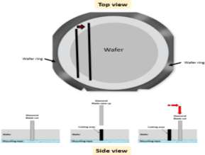
The selection of the single cut technique was based on its inherent difficulty in achieving a balanced performance in terms of topside and backside chipping. However, if single cut wafer dicing is successfully executed, this technique has the potential to provide the most productive process, as indicated by a higher Unit Per Hour (UPH) indicator which is illustrated in “Fig. 7” below. In the evaluation, the same diamond dicing blade was utilised for wafer dicing process to minimize the process variation.

Fig. 7. Single cut illustration.
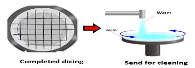
After the completion of the dicing process, the subsequent step involves the initiation of the cleaning procedure for non-UV tape application as illustrated in “Fig. 8”. In the case of using the non-UV mounting tape, after the wafer has completed the dicing process it will be sent for the cleaning process.

Fig. 8. Dicing process on non-UV mounting tape.
However, in the case of a wafer that has been affixed with UV mounting tape, it is necessary to carry out a UV curing process prior to reducing the adhesion of the tape on the wafer surface and wafer backside as well. The UV mounting tape on the wafer surface must be peeled off during the cleaning process as described in “Fig. 9” in order to proceed for the die chipping measurement process.

Fig. 9. Dicing process on UV mounting tape.
4. CONCLUSION
Based on the comprehensive analysis of the collected data, it can be deduced that the utilization action of the novel full sandwich mounting technique can lead to a notable improvement in the chipping performance of silicon dies and simultaneously enhance their flexural strength. Through a comparative analysis between the conventional mounting technique of silicon wafers, with no mounting tape on the wafer surface, and the novel semi and full sandwich wafer mounting technique, wherein mounting tapes were laminated onto the wafer surfaces, it becomes evident that the presence of tape imparts an additional cushioning effect. This effect reduces vibrations during the process of wafer dicing, thereby resulting in a noteworthy reduction in topside and backside chipping performance regardless of the grinding mark patterns.
The flexural strength of silicon dies was studied and found to have an inverse correlation with die-chipping performance after the full sandwich wafer mounting technique was implemented. The successful implementation of full sandwich wafer mounting necessitates careful consideration of the adhesion properties of UV mounting tape. The selection of UV tape should prioritize tape with a high adhesion “before UV curing” specification and a low “after UV curing” adhesion value in order to enhance the performance of chipping and surface peeling test results. The achievement of a minimized silicon die chipping area leads to an enhancement in flexural strength performance. However, further study is required on the usage of the UV mounting on the wafer surface towards full swing of manufacturing condition in order to understand the wafer dicing and wire bonding performance in the longer run. This is because the diamond blade loading during wafer dicing may increase when cutting on the additional layer of mounting tape which adhesive may stick on the diamond blade which may affect the chipping towards the active die circuitry area. The wire bonding process needs further monitoring towards the bonding ability since the concern of mounting tape adhesion remains on the bond pad area. However, the novel double-sided full sandwich wafer mounting technique has given an idea to the industries on how to improve the chipping and the flexural strength performance on the silicon wafers.