SUMMARY
III-Nitride micropillar structures show great promise for applications in micro light-emitting diodes and vertical power transistors due to their excellent scalability and outstanding electrical properties. Typically, III-Nitride micropillars are fabricated through a top-down approach using reactive ion etch which leads to roughened, nonvertical sidewalls that results in significant performance degradation. Thus, it is essential to remove this plasma etch induced surface damage. Here, we show that potassium hydroxide (KOH) acts as a crystallographic etchant for III-Nitride micropillars, preferentially exposing the vertical < 1100 > m-plane, and effectively removing dry etch damage and reducing the structure diameter at up to 36.6 nm/min. Both KOH solution temperature and concentration have a dramatic effect on this wet etch progression. We found that a solution of 20% AZ400K (2% KOH) at 90℃ is effective at producing smooth, highly vertical sidewalls with RMS surface roughness as low as 2.59 nm, ideal for high-performance electronic and optoelectronic devices.
INTRODUCTION
The search for ever smaller electronic and optoelectronic devices has led to numerous innovations. Large planar devices have become micropillars and nanowires,1 allowing aggressive scaling for enhanced functionalities. This paves the way for higher density integrated transistors for more powerful computing, and brighter micro light-emitting diodes (mLEDs) for higher resolution displays for augmented reality (AR) and virtual reality (VR), as well as visible light communication. III-Nitrides including gallium nitride (GaN) offers additional innovations in power electronics and optoelectronics and is a significant research interest due to its wide, direct bandgap, as well as its high electron mobility, and excellent thermal properties. The combination of the material characteristics of III-Nitrides and the use of nanowire and micropillar structures paves the way for the innovation of enhanced GaN-based optoelectronic and power devices,8 such as higher efficiency mLEDs and vertical nanowire or micropillar power transistors.
III-Nitride micropillar or nanowire based electronic and optoelectronic devices can be fabricated through either bottom-up or top-down strategies. In a bottom-up approach, device structures are grown on a substrate through molecular beam epitaxy (MBE) or metalorganic chemical vapor deposition (MOCVD).These growth approaches can result in highly dense forests of individual micropillars or nanowires; however, this unconstrained growth can lead to non-uniformity and coalescence of adjacent pillars or wires. Through the use of a patterned mask on the growth surface, micropillar or nanowire nucleation sites can be intentionally defined, forming ordered arrays of micropillars or nanowires rather than disordered forests.However, non-uniformities between nanowires still limit the effectiveness of these bottom-up approaches.
Epitaxial growth can instead be performed at the wafer scale, enabling a top-down fabrication strategy. In this case, similar MBE or MOCVD epitaxial growth produces layered thin films that can be fabricated into a range of devices and geometries through photolithographic patterning and etching.The use of well-established lithographic processing also offers an extremely high degree of uniformity and control over the placement, size, and geometry of the resulting structures compared to the probabilistic growth of bottom-up fabrication. Etching is typically accomplished using reactive ion etching (RIE) with inductively coupled plasma (ICP) using a Cl2/Ar gas mixture.However, this RIE process also causes crystalline damage in the form of dangling bonds and surface roughness, which form current leakage paths which can severely limit device performance as well as cause nonradiative recombination in optoelectronic devices.

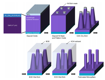
Figure 1. Generalized fabrication process flow for unmasked micropillars.
Several fabrication challenges remain unsolved in this top-down fabrication methodology. GaN is a highly chemically inert material system and the effectiveness of wet etching processes are very limited.Due to this, virtually all top-down GaN fabrication involves one or more dry etch process steps. Dry etching is effective at removing material to form device structures and is a highly mature approach. However, these processes also cause damage to the newly exposed surfaces and typically lead to the formation of nonvertical sidewalls. These defects present challenges for both device fabrication and performance. Slanted sidewalls can complicate subsequent deposition steps, and surface damage due to the dry etch process contributes to nonradiative recombination which significantly reduces the optical output and degrades device efficiency. To optimize device performance, the dry etch damaged III-Nitride micropillar sidewall surface must be fully removed. Therefore, here, we propose an analytical study on the use of KOH-based wet etch that can effectively passivate vertical III-N nanowires and micropillars. This expands upon our previous work which only qualitatively considered etchant temperature. In this work, we investigate the effects of etchant concentration, temperature, and the presence of an insoluble metal mask on the KOH-based wet etching of III-N nanowires and micropillars. The effects of the different etch conditions are analyzed comprehensively, and III-Nitride micropillar sidewall surface roughness was measured and compared from our study.
RESULTS AND DISCUSSION
Background and theory
Several approaches have been investigated to remove or repair dry etch damage and improve overall device performance and efficiency for III-Nitride nano- and microstructures. Passivation through atomic layer deposition (ALD) of dielectrics or treatment with sulfide solutions have been shown to minimize surface recombination, improving device performance and efficiency. Specifically, ALD passivation layers typically provide benefits, such as improved thermal or chemical stability, or can act as optical coating. However, this may require additional time consuming and expensive processing, and will add material to the device surface that can affect the optical properties of the device in the case of optoelectronics such as mLEDs and may not be desirable for power transistors if direct contacts are needed. As an alternative, dilute KOH solutions have also been shown to improve dry etched GaN surfaces for power electronic and optoelectronic devices, such as edgeemitting lasers. Through this KOH method, damaged material at the surface is etched away, removing the current leakage paths and nonradiative recombination centers, thus improving overall device performance for devices such as mLEDs, as demonstrated through improved photoluminescence.21 However, no comprehensive study has been reported yet for vertical III-Nitride micropillars or nanowires. Thus, in this work, AZ400k, a common commercially available photoresist developer is used as the KOH source. This developer contains 2 wt % KOH in solution and is further diluted to 20%, 40%, or 60% AZ400k with deionized water, resulting in an etchant solution with 0.4%, 0.8%, or 1.2% KOH.

Figure 2. Generalized fabrication process flow for Ni masked micropillars.
Experimental
Two sets of micropillars were prepared from an AlGaN/GaN wafer composed of a 0.46 mm layer of Al0.19Ga0.81N atop a 4.7 mm layer of GaN. As shown in Figure 1, fabrication of the first set of micropillars begins by first coating the sample with 500 nm SiO2 via plasma enhanced chemical vapor deposition (PECVD) of tetraethyl orthosilicate (TEOS). Samples were coated with lift-off resist and positive photoresist, then patterned via direct-write lithography. A 150 nm layer of nickel (Ni) was thermally evaporated, deposited and lifted-off. This Ni was first used to mask a fluorine-based plasma etch of the SiO2, revealing the underlying AlGaN surface. The remaining Ni/SiO2 mask was then used to mask a Cl2/Ar etch to form the micropillars themselves. Immersion in HF-containing buffered oxide etch solution dissolved the SiO2, effectively removing the Ni/SiO2 mask. This culminated in the formation of a sparse array of 2 mm tall, 2 mm diameter micropillars with flared bases and sidewalls roughened by the dry etching process.
The second set of micropillars followed a similar fabrication process but omitted the SiO2 interlayer. As shown in Figure 2, after coating the sample with lift-off resist then positive photoresist and identical patterning via direct-write lithography, the same 150 nm layer of Ni was thermally evaporated and deposited directly on the AlGaN surface, and was lifted off. This Ni was used as an etch mask for an identical Cl2/Ar etch, also resulting in similar sparse arrays of flared-base micropillars, with a Ni mask still covering the top surface.
RESULTS
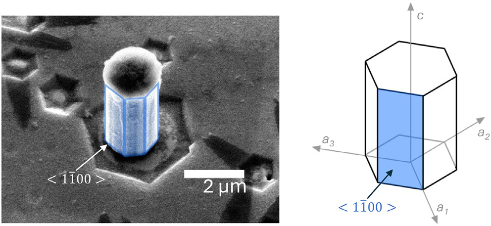
One of the challenges of studying crystallographic etching processes is the need to carefully and precisely align features with the preferentially exposed crystal planes. For these experiments, we selected circular micropillars to avoid the need for this precise alignment and instead rely on the inherent symmetry of the micropillars to allow the structures to effectively self-align crystallographically, as shown in Figure 3. This enables us to analyze and observe the progression and effectiveness of the wet etching process while avoiding the possible unintended introduction of additional sidewall roughness due to crystallographic misalignment.

Figure 3. Micropillar following wet etching showing smooth crystal planes.
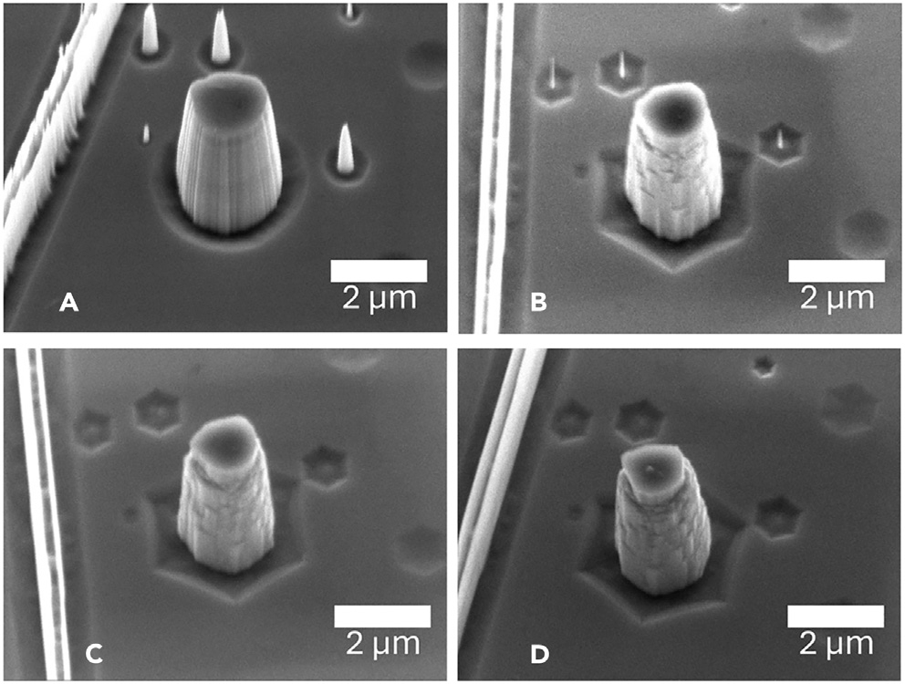
After dry etching in Cl2/Ar, the micropillars were formed with slanted, nonvertical sidewalls that were scored with small vertical grooves, indicative of dry etch damage. This damage is steadily removed during the wet etching process but progresses differently for masked and unmasked structures. For structures without a Ni capping layer, the topmost AlGaN layer etches more quickly than the lower GaN layer. As the wet etch progresses, the diameter of the AlGaN layer steadily reduces, exposing more and more of the c-plane GaN surface at the AlGaNGaN interface. At this newly exposed GaN surface, the KOH etch begins etching downward, revealing the vertical <1100 > plane. However, as this downward etch occurs, the upper AlGaN layer also continues to etch radially inward and further reduce in diameter, exposing additional GaN at the interface. This newly exposed GaN also begins to etch downward, resulting in the formation of numerous steps and terraces down the side of the micropillar, as shown in Figures 4A–4D.

Figure 4. Wet etch progression for micropillars without a Ni mask.
Conclusions
In summary, we have explored the effects of KOH solution concentration and temperature as well as the effects of a metal hard mask on the wet etching of vertical III-Nitride micropillar structures. Solution temperature plays a major role in the observed etch rate, increasing solution temperature from 70℃ to 80℃ causes the observed etch rate to increase from 3.4 nm/min to 24.7 nm/min. Changes in solution concentration have a more minor effect on the initial etch rate, increasing from 20% AZ400K to 40% led to an etch rate increase of only 2.8 nm/min, an increase of approximately 10%. However, as the etch progresses and material damaged by prior dry etching is removed, the etch rate of the underlying undamaged GaN is more sensitive to solution concentration. During the final etch cycle, the same increase from 20% concentration to 40% leads to a dramatic increase in etch rate, rising from 0.8 nm/min to 2.1 nm/min. The presence of a Ni etch mask atop the micropillar has a minor effect on etch rate, but a dramatic effect on post-etch surface morphology. Following the wet etch, samples with a Ni mask showed much smoother, more vertical sidewalls than samples without the Ni mask. Using optimized etch conditions of 20% AZ400K solution at 90℃, micropillar sidewall roughness reduced from 33.09 nm to 2.59 nm after immersion in etchant for 60 min. This reduction in surface roughness is important for the fabrication of III-Nitride laser diodes, enabling the fabrication of smooth, highly reflective etched mirror faces, avoiding the need for mechanical cleaving. Additionally, this wet etch can lead to improved electrical device performance by reducing or eliminating current leakage pathways, essential for III-Nitride transistors and power electronics.
上一篇: 通过全夹层晶圆安装技术改进半导体芯片