Abstract
Silicon Pore Optics (SPO) uses commercially available monocrystalline double-sided superpolished silicon wafers as a basis to produce mirrors that form lightweight high-resolution X-ray optics. The technology has been invented by cosine Measurement Systems and the European Space Agency (ESA) and developed together with scientific and industrial partners to mass production levels. It leverages techniques and processes developed over decades by the semiconductor industry to handle, process, and clean silicon wafers and plates. SPO is an enabling technology for large space-borne X-ray telescopes such as Athena and ARCUS, operating in the 0.2 to 12 keV band, with angular resolution aiming for 5 arc seconds. SPO has also shown to be a versatile technology that can be further developed for gamma-ray optics, medical applications and for material research.
Introduction
The launch of the high-energy astrophysics observatories XMM-Newton and Chandra in 1999 marked the culmination of two major optics development efforts, and made observations of the X-ray sky with unprecedented sensitivity possible. Significant investments were required, and two different optics technologies had to be developed to make these missions possible. The optics of XMM-Newton are based on electro-formed nickel, replicated from precision mandrels. They maximise effective area to make highresolution spectroscopy of distant sources possible. The Chandra optics, on the other hand, optimise the angular resolution at the cost of mass and effective area to provide high-resolution imaging. After more than two decades of active operations, these two missions remain in high demand for their stand-alone capabilities and the synergies with observations at other wavelengths. Their systems are however ageing, and the need for higher performance continues to increase.
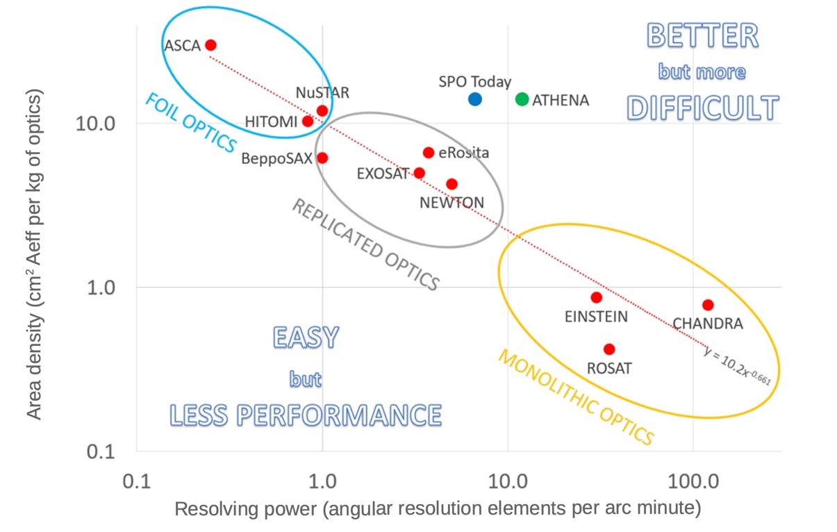
In Figure 1 the optics of these missions are compared, considering the aforementioned three parameters. The area density of the respective optics, expressed as effective area per mass of the optics is plotted against the resolving power of the optics, expressed as angular resolution elements per arcminute. A clear correlation is observed despite the fact that the optics technologies are very different, ranging from foil-based optics to replicated optics and monolithic optics. Each of these systems was developed and built with large effort, and each represents a major achievement, but they all follow a power law correlation. Even the Chandra optics, which are the result of extraordinary efforts in engineering and funding, manage to move only very slightly to the upper right side of the correlation line. The same is true for eRosita, which represents the highly optimised third generation of electroformed nickel technology.

Fig. 1: Characteristics of the optics flown on X-ray missions to date (red dots), plotting the area density of the optics (i.e. cm2 of effective area per kg of optics) as function of the resolving power of the optics (i.e. number of angular resolution elements resolved by the optics in one arcminute). The characteristics of the X-ray optics flown to date show a clear correlation, described by a power law. Athena requires optics which cannot be achieved with the X-ray optics technologies flown to date. Adapted from.
The graph illustrates that lightweight optics with large effective area but lower angular resolution, or high resolution but heavy optics with a limited effective area have been built until now. Current optics-making technologies have so far allowed for the production of systems where only two of the three parameters can be effectively optimized at one time. The optics for the Athena mission (green dot in Figure 1) however require a technological change to move away from this empirical power law into the ‘difficult corner’ to the upper right of the graph. Linear extrapolation of all the X-ray missions flown to date using the three previous conventional technologies suggests that it would be possible to deliver the resolution and effective area, but it would require a mass of about 7000 kg, which is the mass of the complete Athena mission. Or it could respect the mass allocation of 1000 kg and deliver the effective area, but with a severely degraded angular resolution of about 1.6 arcminutes.
SPO concept
SPO technology uses commercially available monocrystalline double-sided super-polished silicon wafers as a basis to produce X-ray mirrors. In addition to its direct bonding property, silicon is rigid, has a relatively low density, and a very good thermal conductivity. Silicon wafers have excellent surface finish, both in terms of figure and surface roughness, making them a superb base material to build X-ray mirrors.
SPO development leverages the massive investments done in the semiconductor and automotive industries, which made available high-performance equipment, tools, materials and processes allowing highquality mass production. The work-horse of the semi-conductor industry are thin 300-mm wafers sawn out of monocrystalline ingots, grown from poly-crystalline silicon using the Czochralski method. These wafers are produced with outstanding quality for a modest cost: prime grade double-sided super-polished monocrystalline 300 mm silicon wafers have specifications of 0.1 nm root mean square (RMS) surface roughness and total thickness variation (TTV) of less than 0.2 µm (see Figure 2).

Fig. 2: Typical relative thickness map of a silicon wafer for SPO plate production. The data is plotted relative to the median thickness of 775110 nm of the wafer. The thickness is measured by Fizeau interferometry. Credit: cosine.
Potential and limitations of SPO
In this section, we discuss the potential and limitations of the SPO technology in general terms. For Wolter I geometry, three aspects are discussed: the plate minimum and maximum lengths, the radial spacing between mirror plates, and the smallest sagittal radius that can be achieved.
Thinner wafers are produced in smaller series and present higher roughness and larger thickness variations than the standard 300 mm ones, which has until recently made them less attractive to use. However, some of these defects can be eliminated with the use of ion beam figuring (IBF), which now offers a way to reduce thickness variations and reduce roughness (see Section 4.1). Thus, it is possible to think of SPO with mirror plate pitch smaller than 0.775 mm. At the other end, it would also be possible to bond wafers together and then process them. This opens the possibility to create stacks of mirror plates with doublepitch of 1.55 mm. This would be useful in case of large incidence angle, where the plate length would become too short otherwise.
SPO realization
Production of SPO mirror plates
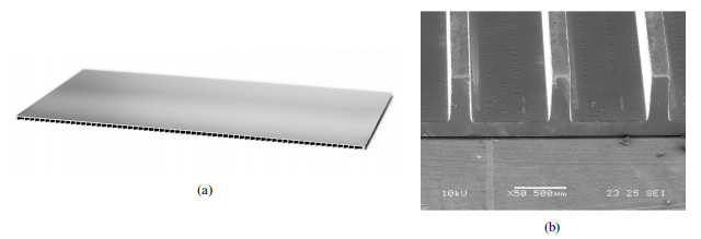
With the technology contributions from the semiconductor industry, mass production is being set up and standardized processes are being developed in order to manufacture SPO mirror plates in high quality, large quantity, and at relatively low cost . The production of SPO mirror plates starts with carving out ribs into 300 mm wafers. This process is effectively performed by removing material from the wafer down to the desired membrane thickness. Subsequently, rectangular plates are diced off the wafer, with the ribs along the direction of travel of the X-rays. The orientation of plate ribs and edges is aligned with a crystal plane of the silicon to ensure correct bending, as well as chemical processing properties of the material in subsequent production steps. The top side of the mirror plate is the reflective side (Figure 4, a)) and the bottom is the ribbed side (Figure 4 b)) with the ribs parallel to each other. The plates currently manufactured have rib pitch varying from 1.0 mm to 2.4 mm with rib width of 0.17 mm.

Fig. 4: (a) Example of a SPO mirror plate with its reflective side on top, and ribbed side facing down. (b) Scanning electron microscope image of the ribs of a SPO mirror plate. Credit: cosine.
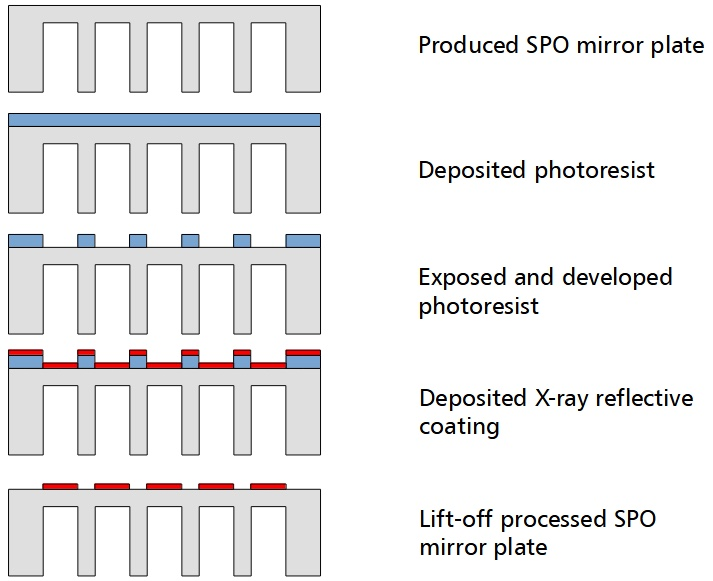
The SPO mirror plates feature a patterned coating on their reflective side in order to enable direct silicon bonding (see Section 4.4). The patterning of the coating is performed via optical lithography. This process, sketched in Figure 5, consists of the following steps. Firstly, a photosensitive polymer is deposited on the reflective side of the SPO mirror plate. In a second step, a patterned photoresist layer is created by exposing the photosensitive polymer to ultraviolet light and developing it by immersing the sample in a chemical solution. Subsequently, an X-ray reflective coating is deposited using a sputtering deposition technique. Finally, chemical lift-off is performed to remove the coated photoresist resulting in a patterned coated SPO mirror plate.

Fig. 5: Schematic of optical lithography for SPO mirror plate with patterned X-ray reflective coating. Credit: cosine.
Summary and conclusions
SPO uses technology developed over multiple decades by the semiconductor and automotive industries, which have massively invested in the fabrication and processing of silicon wafers. It has become a very mature technology, thanks to the continuous development efforts to prepare the industrial production of the largest X-ray optics yet to be launched into space. SPO is an enabling technology for Athena, and is ontrack for meeting the observatory’s ambitous requirements for effective area, angular resolution, and mass. The optics for Athena are under intense development, aiming to start the manufacturing the first flight MMs in 2026. In parallel, facilities for the assembly and testing of the MMs, co-alignment of the MMs in the MA, and ground calibration of the MA are being implemented.
上一篇: 半导体制造中的多级过程诊断网络