ABSTRACT
The semiconductor industry, driven by technological advancements, is continuously undergoing process micronization. This micronization has led to an increased complexity in the wafer fabrication process and equipment. Inevitably, this change leads to a rise in defect rates. Furthermore, the traditional manual analysis methods for these defects possess several limitations. Notably, the defect analysis process is time-consuming and heavily relies on the expertise of the workers, making it challenging to achieve consistent analysis results. In modern semiconductor manufacturing sites, a vast amount of sensor data is being generated in real-time from various equipment. These sensor data contain information on the wafer’s condition, the progress of the process, and the operating conditions of the equipment. The purpose of this study is to examine the use of this sensor data in creating a deep learning model that leverages information generated within multi-stage manufacturing processes. The proposed method is designed to automatically classify the defect status of wafers and interpret the causes of these defects. Using the sensor data from two process equipment in semiconductor manufacturing, we achieve better classification performance than other existing methods. Through the interpretation of the classification results, we can identify the sensors and equipment that significantly impact the classification results. The proposed methodology is expected to significantly reduce the effort and reliance on engineers for defect analysis, thus greatly improving production efficiency.
I. INTRODUCTION
Recent advancements in semiconductor processing micronization have led to increased complexity in processes and equipment, with some products which undergo hundreds of process steps. Furthermore, as the Internet of Things, smartphones, and artificial intelligence sectors gain attention, the application areas for semiconductors are expanding, consequently leading to a surge in demand.
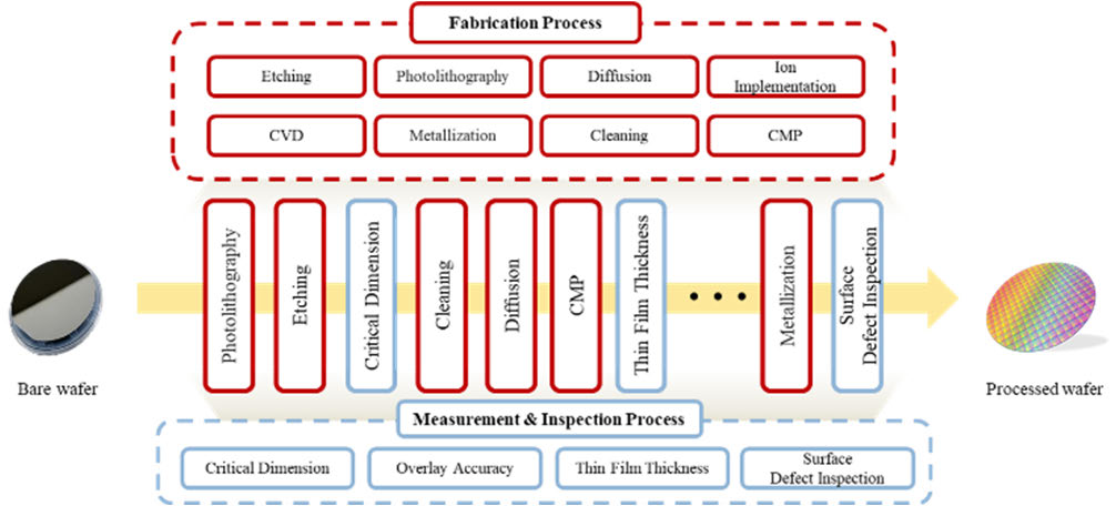
Figure 1 shows that semiconductor manufacturing begins with the input of a bare wafer and is completed as a final product after undergoing complex processes. This procedure is broadly divided into wafer fabrication and measurement and inspection processes. The wafer fabrication process is based on eight detailed sub-processes. These include the etching process for surface patterning, photolithography for circuit formation on the surface, diffusion and ion implantation processes for imparting electrical properties to the wafer, chemical vapor deposition (CVD) and metallization processes for forming thin films and providing conductivity, and cleaning and chemical mechanical polishing (CMP) processes for wafer surface refinement. On the other hand, the measurement and inspection processes involve critical verification tasks such as measuring circuit line widths (critical dimension), assessing the alignment of layers (overlay accuracy), measuring the thickness of thin films, and inspecting surface defects. After undergoing these various processes, the wafer is finally packaged and completed as a product.

FIGURE 1. An example scenario for obtaining a processed wafer in the semiconductor wafer manufacturing process. Both the fabrication and inspection processes are carried out over hundreds of steps.
In such complex production processes, various methods are implemented to monitor the manufacturing process to maintain production volume and quality. Particularly, defects arising during the wafer fabrication process are one of the major issues. After undergoing multiple stages of processing, wafers are inserted into inspection equipment to check their processing status. This inspection process is usually limited to a subset of wafers, and confirming the results can take from a few minutes to several hours. If defects are detected in a wafer, an investigation is conducted to determine at which process stage the defect occurred. This investigation process typically takes a considerable amount of time and heavily depends on the expertise of engineers.
II. RELATED WORKS
Reflecting the trend of increasing sensor data availability and computational power in the semiconductor manufacturing field, deep learning methodologies are being actively applied to equipment data. Particularly, studies on wafer defect detection using SVID, which best represents equipment status, have been extensively conducted. Convolutional neural network (CNN), predominantly used in the image domain, was applied by to classify wafer status into six categories using multivariate time-series data, SVID. Reference investigated using a CNN to classify semiconductor wafer particle defects by combining scanning electron microscopy (SEM) images with energy-dispersive x-ray (EDX) data. This approach aimed to reduce analysis time and human error, significantly enhancing classification performance and enabling more efficient defect source analysis.
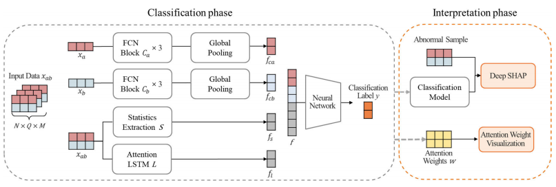
Figure 2 illustrates the overall structure of the proposed MP-DN. The dataset used in the experiment is multivariate time-series, defined as a tensor of shape (N, Q, M). Here, N is the number of samples in the dataset, Q is the length of the time-series, and M is the number of variables. This tensor, denoted as xab, serves as the input to the network.

FIGURE 2. Overview of the proposed MP-DN consisting of the classification and interpretation phases.
IV. EXPERIMENTS
In assessing the performance of the classification model, accuracy and F1-score were used as evaluation metrics. Accuracy is an indicator of how correctly the model classifies the entire dataset, calculated as the ratio of samples correctly classified out of the total samples. The F1-score is calculated as the harmonic mean of precision and recall. Precision is the ratio of instances that are actually ‘‘normal’’ among those classified as ‘normal’ by the model. Recall is the ratio of instances classified as ‘‘normal’’ by the model among the actual "normal" instances. Given the class imbalance in the data, additional evaluation metrics such as the F1 macro score and the Matthews correlation coefficient (MCC) were used. The F1 macro score is used in binary classification to represent the average of the F1 scores calculated for each class, making it a useful metric when considering class imbalance. The MCC is a measure in binary classification that considers class imbalance and evaluates performance, ranging between −1 and 1. A score close to 1 indicates perfect prediction, close to 0 indicates random prediction, and close to −1 indicates perfect inverse prediction.
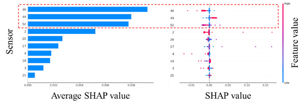
Figure 3 presents the results interpreted through deep SHAP for cases classified as ‘’abnormal "by the model. From Figure 3, it was evident that Sensors 46, 44, and 52 significantly influenced the model’s defect detection. Specifically, Sensor 44 tended to lead to an ”abnormal" classification when it had high values, whereas Sensors 46 and 52 tended to lead to a“normal” classification under similar conditions. Furthermore, considering that Sensors 46, 44, and 52 are sensors of the Process B equipment, it could be inferred that Process B significantly influences the classification of ‘‘abnormal.’’

FIGURE 3. An example of interpreting the classification results obtained by deep SHAP. Sensors 46, 44, and 52 have a greater impact on the results compared to other sensors.
V. CONCLUSION
Current developments in semiconductor manufacturing processes have resulted in more intricate procedures and equipment because of the ongoing trend of micronization. In addition to this, the demand for semiconductor chips in various sectors like the Internet of Things, mobile devices, and artificial intelligence has surged, creating a greater demand for increased efficiency in semiconductor production facilities. Maintaining high productivity necessitates minimizing wafer defects and ensuring rapid response to such incidents. Efforts are in progress across various sectors to leverage the rich data collected from the myriad of sensors installed in equipment. While there is a significant body of research using deep learning to detect wafer defects through equipment sensor data, the practical application in multi-stage process scenarios frequently encountered in real-world settings remains limited. This study introduces MP-DN, a deep learning model designed for classifying and interpreting wafer defects based on multi-stage process equipment sensor data. Our experiments, conducted against various comparative models, have demonstrated that the proposed model delivers superior performance in multi-stage process equipment sensor datasets. By incorporating deep SHAP and attention mechanisms, the model classifies and interprets the results, paving the way for its application in subsequent defect analysis engineering tasks. Implementing this study in actual field conditions is anticipated to significantly reduce the time required for analyzing wafer defects and to provide vital clues for defects, thus enhancing the efficiency of subsequent defect analysis engineering and, ultimately, raising the productivity of semiconductor factories. Meanwhile, while this study assumes that all data is labeled, in reality, labeled data is often scarce relative to the available data. Future research will explore robust classification performance using equipment data-driven self-supervised or semi-supervised learning methodologies in environments with limited labeled data.
下一篇: 硅孔光学器件