Abstract.
Electrostatically tunable Josephson field-effect transistors (JoFETs) are one of the most desired building blocks of quantum electronics. JoFET applications range from parametric amplifiers and superconducting qubits to a variety of integrated superconducting circuits. Here, we report on graphene JoFET devices fabricated with wafer-scale complementary metal-oxide-semiconductor (CMOS) compatible processing based on wet transfer of chemical vapour deposited graphene, atomic-layer-deposited Al2O3 gate oxide, and evaporated superconducting Ti/Al source, drain, and gate contacts. By optimizing the contact resistance down to ~170 Ωµm, we observe proximity-induced superconductivity in the JoFET channels with different gate lengths of 150–350 nm. The Josephson junction devices show reproducible critical current IC tunablity with the local top gate. Our JoFETs are in short diffusive limit with the IC reaching up to ∼ 3 µA for a 50 µm channel width. Overall, our successful demonstration of CMOS-compatible 2D-material-based JoFET fabrication process is an important step toward graphene-based integrated quantum circuits.
Introduction.
The progress in studying mesoscopic physics and topological superconductivity, as well as applications of quantum information processing with proximized semiconductor-superconductor hybrid devices, has thus far been mostly limited to chipscale fabrication. The graphene devices have been identified among the most promising candidates for realizing Josephson junctions (JJs) including exfoliated boron-nitrideencapsulated graphene,III-V and groupIV two-dimensional electron gas heterostructures,and nanowires. A particular attention has been focused on the development of Josephson field-effect transistors (JoFETs) where the proximity-effect-based supercurrent is controlled by an electrostatic gate electrode. JoFETs enable a wide range of applications such as quantum coherent electronics, quantum memories, classical digital superconducting electronics, ultra-sensitive bolometers, and quantum-limited parametric amplifiers.
After graphene JJs are probed at 300 K, the wafer is diced, and selected samples are cooled down in a dilution refrigerator with a base temperature of Tbase = 42 mK. DC and low-frequency lock-in measurements (ac current excitation is 35 nArms at 33.3 Hz frequency) are carried out for the devices wire-bonded in two or four-probe configurations. In the former case, the wire resistance is digitally subtracted.
Results and discussion.
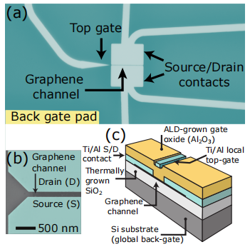
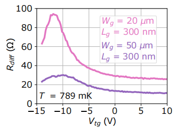
The optical and scanning-electron-microscope (SEM) images of the final top-gated JoFET, similar to those measured in this paper, are shown in Fig. 1 (a,b). A schematic cross-section of the JoFET is given in Fig. 1(c). Fig. 2 shows the normal-state differential resistance vs top-gate voltage characteristics Rdiff(Vtg) with an on/off ratio of ∼ 3–4 for two JoFETs with gate length Lg = 300 nm and width of Wg = 20 µm and 50 µm, respectively.

Figure 1: (a) False-color optical microscope image of a JoFET in a four-probe configuration (b) False-color SEM image of the channel with length Lg = 150 nm between the source and drain electrodes, taken before gate deposition. (c) Three-dimensional schematic of the JoFET.

Figure 2: Normal-state differential resistance Rdiff as a function of top-gate voltage Vtg for two JoFETs at Vbg = 0.
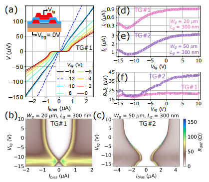
The current–voltage characteristics of the top-gated device with Lg = 300 nm and Wg = 20 µm are shown in Fig. 3(a) for different Vtg at 42 mK. The lock-in measurements of Rdiff as a function of Ibias and Vtg for devices TG#1, 2 from Fig. 2 are shown in Fig. 3 (b,c). At the same time of acquiring differential resistance 2D maps, we were measuring the gate current leakage, and found that it was below 1 nA (setup limit) for the entire Vtg range between +10 V and −15 V. The critical current extracted from Fig. 3(b,c) as a function of Vtg is shown in Fig. 3(d,e). The IC values extracted for positive and negative Ibias were symmetric. While for TG#1, the coherent transport is almost entirely suppressed at VDir, the wider device, TG#2, has a superconducting plateau which does not close due to the channel inhomogeneity, similar to what has been reported in. Despite the difference close to VDir in suppression of supercurrent, for fixed Lg, the IC ratio at Vtg = 10 V, 3 µA/0.9 µA = 3.3, approximately matches the Wg ratio 50 µm/25 µm = 2.5. For the third device, TG#3 with Lg = 200 nm and Wg = 20 µm, at Vtg − VDir ≈ 10 V and Vbg = 0, we find IC = 1.1 µA (see Supplementary material), confirming a good scaling of IC with geometrical parameters of JJs.

Figure 3: (a) Measured voltage across the junction V as a function of direct-current bias Ibias for T = 42 mK and the indicated top-gate voltages Vtg (device TG#1). Inset shows a simplified device sketch and gate-biasing configuration. (b,c) Measured differential resistance Rdiff as a function of Vtg and Ibias for two JoFET devices with Lg = 300 nm and (b) Wg = 20 µm and (c) 50 µm. (d,e) Critical current IC extracted from (b,c) as a function of Vtg, respectively. (f) The product of the critical current and normal-state resistance ICRN calculated from (b,c).
Conclusion and Outlook.
In summary, we have demonstrated 150-mm-wafer scalable fabrication of JoFETs with low contact resistance using CVD graphene and the local top gate control. We observe field-effect-tunable critical current up to a few µA, shown to have reasonable scaling with gate length and channel width. Our JoFETs operate in the short diffusive regime as measured for seven devices at low temperatures. Operated in the overdamped regime, our devices have a good stability against thermal cycling.
Our JoFETs are fabricated similarly to conventional CMOS-compatible CVD-graphene FETs and our 300K-wafer-scale device yield exceeds 90%. As the next milestone, we aim to reduce the Lg down to 50 nm, optimize the position of VDir, and improve the junction transparency toward the wafer-scale realization of graphene quantum integrated circuits such as superconducting quantum interference devices, RF switches and multiplexers. Our process allows to combine normal-state and superconducting FETs on the same chip to explore the hybrid electronics at the circuit and system design level, with energy-efficiency improved by the ambipolar behavior of graphene normal-state and superconducting FETs. Alternatively, the heterogeneous integration of graphene JoFETs with commercial CMOS can be envisioned, similar to Ref.
下一篇: 碳纳米管集成电路技术:纯化、组装和集成