Abstract
As the manufacturing process of silicon-based integrated circuits (ICs) approaches its physical limit, the quantum effect of silicon-based field-effect transistors (FETs) has become increasingly evident. And the burgeoning carbon-based semiconductor technology has become one of the most disruptive technologies in the post-Moore era. As one-dimensional nanomaterials, carbon nanotubes (CNTs) are far superior to silicon at the same technology nodes of FETs because of their excellent electrical transport and scaling properties, rendering them the most competitive material in the next-generation ICs technology. However, certain challenges impede the industrialization of CNTs, particularly in terms of material preparation, which significantly hinders the development of CNT-based ICs. Focusing on CNT-based ICs technology, this review summarizes its main technical status, development trends, existing challenges, and future development directions.
1. Introduction
Over the past half-century, the chip industry has progressed significantly due to Moore’s law (the integration of chips doubling every 18 months), which has profoundly changed the pattern of people’s lives and industries. During this transformation, the rapid iteration of new technologies constantly refreshes the technical nodes of Si-based chips, thereby surpassing Moore’s limits in several cases. However, in the second decade of the 21st century, the development speed of the chip process decreased significantly, mainly because the scale of Si-based field-effect transistors (FETs) approached the physical limitations. Currently, benefiting from advanced technologies such as extreme ultraviolet lithography, the mature manufacturing process has entered the 4 nm technology node, and the industry is evolving to the 3 nm or even 1 nm node. Each step forward incurs significant costs and requires a longer time to understand the core technologies. Moreover, merely relying on enhancing manufacturing techniques to improve the performance of Si-based chips cannot fully satisfy the current demands.
According to the latest International Technology Roadmap of Semiconductor (ITRS), the short-channel effect becomes increasingly concerning as the technology node approaches its physical limits, as it results in the failure of microelectronic devices to follow the principles of traditional semiconductor physics. Hence, the potential of Si-based chips is almost exhausted, and Moore’s law is no longer applicable. New materials and manufacturing methods are internationally recognized methods for fundamentally solving problems associated with chip performance, whereas carbonbased semiconductors are considered disruptive technologies in the post-Moore era.
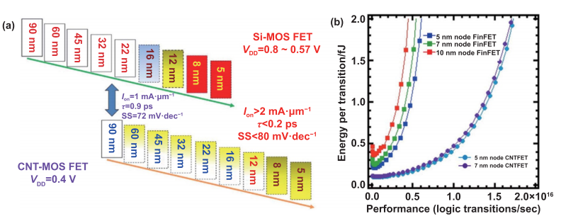
Furthermore, researchers reported that CNT-based FET (CNT FET) significantly improved electrical performance and energy consumption compared with silicon. For Si-based FETs scaled from 7 nm to 5 nm, the corresponding chip performance increased by approximately 20% (figure 1). By contrast, the performance of CNT-based chips under 7 nm technology nodes is three times higher than that of Si-based chips, which is equivalent to the improvement of the 15th generation of the latter; therefore, academics predict that the dominance of the Si chip industry will be terminated by the utilization of CNTs.

Figure 1. Comparison of Si and CNT FET. (a) Transistor technology comparison of Si and CNT FET roadmaps. (a) Reprinted from , Copyright © 2014 Elsevier Ltd. (b) Energy vs. performance of current FinFET and future CNT FET technologies. Reprinted with permission from [30]. Copyright (2014) American Chemical Society.
2. Preparation of s-CNTs with high purity and high yield
The intrinsic properties of CNTs are affected significantly by their chirality. Structurally, CNTs can be viewed as a single sheet of graphite seamlessly curved along a certain direction to form a tubular structure. And the chiral coefficient (n, m) characterizes the wrapping direction and determines the size of the wrapping angle. Due to the fact that different electronic properties exhibited by CNTs strongly depend on the wrapping angle, researchers typically use chiral coefficients to characterize certain types of CNTs. Specifically, when n = m, CNTs have bands crossing the Fermi level and are therefore metallic. And these particular CNTs are called armchair tubes. The remaining types exhibit two possibilities. When n–m = 3 l (where l is an integer), tubes are also expected to be metallic. In the case n–m = 3 l, tubes are predicted to be semiconducting.
Generally, high-quality s-CNTs are mainly purified via chemical vapor deposition (CVD) and solution methods. Research shows that chirality-specific CNTs can be synthesized via CVD, but the chiral purity is far from meeting the current requirements of VLSI manufacturing. Moreover, based on the results achieved in existing research, the solution method has already taken the lead. Solution methods can be classified into three main categories: aqueous systems based on surfactants, organic systems based on polymers, and aqueous two-phase systems. The solution method offers significant advantages for the preparation of ultrahighpurity s-CNTs and is expected to benefit CNT-based VLSI manufacturing.
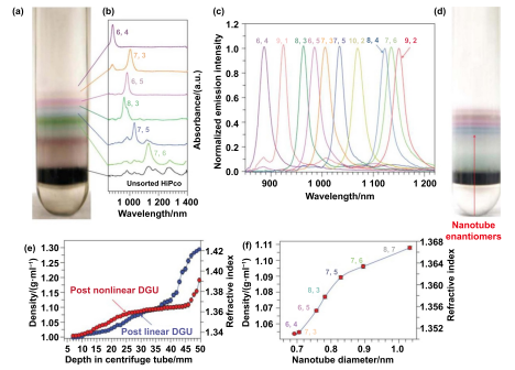
Surfactants such as sodium dodecyl sulfate (SDS) and sodium dodecyl benzene sulfonate (SDBS) can effectively disperse CNTs in aqueous solution. Notably, surfactants exhibit extremely low selectivity for different types of CNTs. After suspension formation, density gradient ultracentrifugation (DGU) or column chromatography is generally performed to further purify CNTs. Arnold et al first used the DGU method to classify CNTs , where single-stranded DNA and iodine octanol were used as the surfactant and density gradient medium, respectively. Under a long duration of high-speed centrifugation, the CNTs were layered in the solution based on their diameters. This study achieved a high purification efficiency for small-diameter s-CNTs, and the chiral types were (6,5), (9,1), and (8,3). Subsequently, Weisman’s group improved the DGU method using a customized S-shaped gradient centrifuge tube, as shown in figure 4. This centrifuge tube had a very shallow gradient and was nonlinear. Under the action of an ultrahigh centrifugal force, even CNTs with insignificant chirality differences can be separated, thus significantly improving the resolution accuracy of the chirality. Using this method, researchers extracted up to 10 types of chiral s-CNTs from HiPCo carbon tubes, with diameters ranging from 0.7 nm to 1.1 nm and the highest purity of 88%.

Figure 4
5. Conclusion and prospect
Currently, the development of CNT-based chip manufacturing technology has indicated significant achievements; however, main obstacles must be broken through before s-CNTs can be industrialized. To surpass the performance of Si-based chips, CNT-based chip technology should be further developed as follows: (1) the preparation of high-quality and high-yield s-CNTs. In this respect, the solution method is preferred. The purity of s-CNTs prepared using the polymer purification method exceeds the 99.999 9% standard required for large-scale ICs. Moreover, for the same technology node, the state performance of CNT-based FETs surpasses that of Sibased FETs. However, this ultrahigh purity was achieved at the expense of production yield. Although an increase in the number of process steps improves the quality, it also significantly increases the manufacturing cost, which does not provide a competitive advantage. In the future, the development of CNTbased technology should be low cost. (2) Reliable large-scale fabrication of aligned CNT arrays. High performance CNTbased transistors impose strict requirements on the arrangement of CNTs in the channel, that is, to achieve a high density (>125 tube·µm−1 ) while ensuring reasonable spacing (5 nm). To manufacture ICs, hundreds of billions of CNTs must be arranged in a highly ordered manner on a macro scale. Existing methods of DNA and pull-up assemblies satisfy these requirements; however, the repeatability and stability must be improved. (3) Establishment of technological process standards for CNT-based ICs. We think that this section is based on overcoming material challenges and forming a uniform technological process to achieve device homogeneity and stability preparation. Currently, the manufacturing process for highly integrated CNT FETs is not consistent in many works, especially the unique cleaning, CMOS doping, and electrode contact process steps of CNTs. In the future, new technologies need to be broken through to apply to smaller CNT FET nodes, such as CNT-BNNT heterostructure nanotube and high k gate dielectric materials], to solve the contact and gate control issues of extremely scaled devices.