Numerous parameters are regulated in the wet chemical oxidation process for TOPCon/POLO solar cell technology to improve silicon oxide passivation (SiO2 ). Understanding the electronic properties, particularly the lifetime of the carriers and their thickness, requires knowledge of the properties of the surface of crystalline silicon (c-Si), which is subjected to native oxide etching, followed by wet chemical oxidation, such as nitric acid or hot water oxidation and various hydrogenation methods. The results of these processes are tracked with lifetime measurement equipment, and spectral ellipsometry is used to measure the thickness of the oxide layer by using the single-sided polished wafers with surface orientation (1 1 1). In addition to the actual values, their time stability is also tracked. Before the hydrogenation step was introduced, the wafers’ lifetime was approximately 0.001 ms, which is less than the bulk lifetime; with the hydrogenation, the lifetime increased by more than an order of magnitude for a relatively long time with no difference between (1 1 1) and (1 0 0) wafers indicating that hydrogenation of the Si/SiO2 interface is performed.
INTRODUCTION
Silicon is the finest material for creating a solar cell for two key technological reasons. Primarily, it is the second most abundant material, and secondly, it has a permanent oxide layer that provides excellent electrical insulation. Furthermore, the low defect density at the Si/SiO2 interface makes it ideal for electrical applications. To produce the desired SiO2 layer, various oxidation methods such as thermal oxidation, wet chemical oxidation and plasma-enhanced oxidation are commonly used. Each approach has its benefits, and the best one is chosen depending on the particular needs of the semiconductor fabrication process, e.g. thermal oxidation is at least as good as wet chemical oxidation.
The wet chemical oxidation of silicon has a long history that began in the 1950’s with the development of semiconductor technology. Researchers at that time were investigating several techniquesfor growing oxide layers on silicon substrates. One of the early methods required heating silicon wafers to temperatures above 800℃ while exposing them to a combination of water vapour (H2 O) and oxygen (O2 ), commonly called dry oxidation. This approach produced high-quality oxide layers but required high temperatures and prolonged processing times. Various liquid oxidants, like nitric acid and hot water, are introduced to avoid long processing times, resulting in a faster and more controlled oxidation process. The nitric acid (HNO3 ) oxidation of silicon produces silicon dioxide (SiO2 ) and other by-products. The depth and nature of the oxide layer that forms on the silicon surface depend on the temperature and length of the immersion. HNO3 oxidation isfrequently combined with other techniques, such as dry/steam oxidation.
EXPERIMENTAL
Czochralski M2 (156.75x156.75mm2 ) n-type wafers with a base resistivity of 2.25 Ω cm and bulk lifetime of around 1 ms from Longi solar were laser cut into 50 mm circular wafers. The wafers are categorised into two surface orientations, i.e., (1 0 0) after saw damage etch and (1 1 1) textured by KOH solution. The (1 1 1) wafers are transferred into an automated wet bench for cleaning, etching the native oxide (SiO2 ) layer, and for wet chemical oxidation. The two steps of RCA (Radio Corporation of America) cleaning procedure SC-1 and SC-2 are performed. SC-1 etch composed of NH4 OH (28 - 30%), H2 O2 (30 %), and deionised (DI)-water(18.2 MΩ cm) in proportions of 1:1:5 is used at room temperature for 10 minutes to remove the organic residues.
As a result of HNO3 oxidation, a thin layer of SiO2 is formed. On half of the wafers, the additional wet hydrogenation step is performed. On the other half, the dry hydrogenation process is carried out. The overview of the experimental conditions is shown in Table 1. The carrier lifetime of a pair of wafers is measured for each combination. During each experimental step, single-side polished wafers with orientation (1 1 1) are used to measure the thickness of the SiO2 layer (see Table 2) by spectral ellipsometry by J. A Woolam 2000 ellipsometer.
The photoconductivity for the reference wafer is shown in Fig. 1. The reference wafer (polished p-type wafer) has a thickness from 500 to 550 µm and a base resistivity from 1 to 10 Ω-cm is used to determine the photoconductivity. The photoconductance (Siemens) and light intensity (suns) asfunctions of time are shown in Fig. 1(a). The Quasi Steady State Photoconductance (QSSPC) method is being used. The light intensity must be smooth and exponentially decaying in order to determine the sample’s effective lifetime. Fig. 1(b) displays the carrier lifetime as a function of excess carrier density. The graph measures the carrier lifetime at the provided carrier density, the carrier density may vary depending on the method utilised in calculating the lifetime.
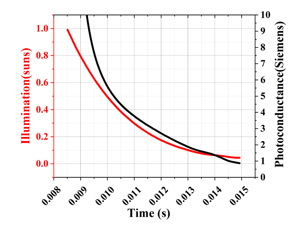
Fig. 1(a). Represents the photoconductance and Illumination with respect to time.
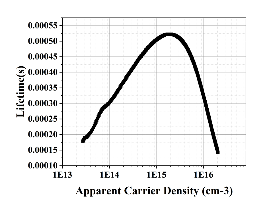
Fig. 1(b). Represents the lifetime with respect to carrier density.
RESULTS AND DISCUSSION
Following the RCA cleaning process, Fig. 2 illustrates the effect of two different etching techniques performed on the (11 1) and (100) oriented wafers. Irrespective of the wafer orientation, Fig. 2 shows that the surface passivation is considerably higher immediately after HF etching and nitrogen drying than NH4 F etching. After roughly one day,τeff dropsto values around 2µs. The impact of different etching techniques on the wet chemical oxidation is shown in Fig. 3. In the current instance, the carrier lifetime is all similar with a weak trend of slightly higher values for the (111) oriented wafers in HF etching solution. This is due to the high etching rate, selectivity, and uniformity of HF etching. To understand the HNO3 (65 wt. %) oxidation temperature effect, an optimisation experiment is performed with the oxidation time kept constant, and the results are presented in Fig. 3. The trend indicates that the oxidation performed at 100°C gives the best carrier lifetime.
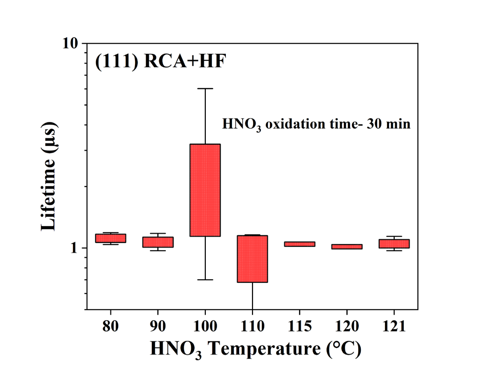
Fig. 3. Effect of different oxidation temperatures on HF etched wafers.
However, looking at Fig. 4, whether the quality of oxide passivating is questionable. In the reality of TOPCon or POLO technology, the silicon oxide is combined with field effect passivation provided by a doped polycrystalline layer and also by hydrogenation step provided by deposition of SiNx layer from silane/ ammoniac mixture and firing. An original procedure of wet hydrogenation is carried out to provide hydrogenation. The wafers that underwent the wet hydrogenation procedure have a much longer carrier lifetime than those obtained immediately after the HNO3 or H2O oxidation process.
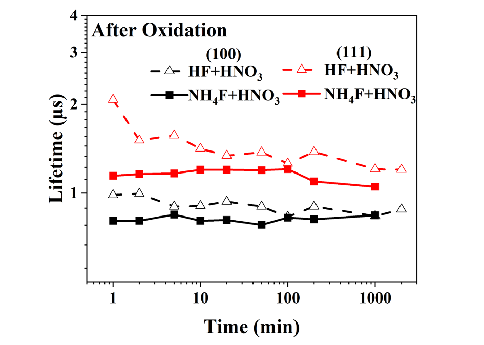
Fig. 4. Effect of HNO3 oxidation on HF and NH4 F etching process.
Alternatively, to the wet hydrogenation, we used dry hydrogenation by SiNX:H layer, deposited by Plasma Enhanced Chemical Vapor Deposition (PECVD) and firing at 800°C at a speed of 470 cm min-1. Hydrogen in the SiNx:H layer diffuses towards the Si/SiO2 interface. As shown in Fig. 7 and Fig. 8, dry hydrogenation gives a considerably higher carrier lifetime that is perfectly stable in time. The stability is most likely provided also by the SiNx capping layer. Figs. 7 and 8 illustrate the effect of the HF vs. NH4 F etching process before the HNO3 oxidation. We can observe that the wafers that underwent HF etch always have a higher carrier lifetime than those that are NH4 F etched.
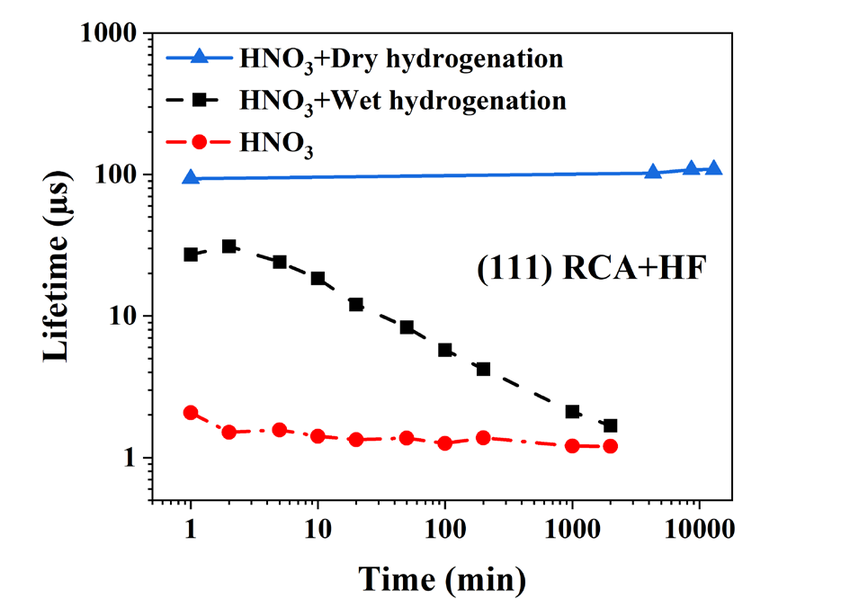
Fig. 7. Effect of HF etching on dry, wet hydrogenation and HNO3 oxidation.
CONCLUSIONS
The carrier lifetime following HNO3 and H2 O oxidation is relatively low, which suggests that the SiO2 layer produced is highly defective. An original process of wet hydrogenation after oxidation, when tested against the standard dry hydrogenation process, the carrier lifetime was more than an order of magnitude higher than the carrier lifetime obtained after HNO3 and H2 O oxidation. Interestingly, the carrier lifetime value does not depend much on the type of native oxide etching and the surface orientation but strongly depends on the method of re-oxidation. Another benefit of wet hydrogenation is the carrier lifetime’s temporal stability, which is considerably improved, especially for the HF etched Si (111) surface, which is probably the most relevant for future industry. Furthermore, when using standard dry hydrogenation, it is observed that H2 O oxidation gives almost an order magnitude higher values when compared to the wafers that underwent HNO3 oxidation. This is quite the opposite of the wafers that underwent wet hydrogenation after HNO3 and H2 O oxidation. It can be concluded that in the case of dry hydrogenation, irrespective of the HF or NH4 F etch, water oxidation is the most suitable process to grow the oxide layer. This high lifetime stability provides the benefit of using the textured wafers on the rear side of the TOPCon structures.
下一篇: 异质蓝宝石支撑的低损耗光子平台