This paper reports on a fabrication process suitable for ultra-low resonant frequency inertial MEMS sensors. The low resonant frequency is achieved by electrically tunable springs and a heavy mass formed by through-silicon deep reactive-ion etching (DRIE) applied to a silicon-on-glass. A thermal issue of through-silicon DRIE (TSD) stemming from the low-resonant-frequency structure is circumvented by two methods: introducing cooling time between the DRIE steps, and adopting a metal hard mask. A blade dicing method suited for this process is also presented. To monitor the verticality of TSD, a non-destructive taper detection method that utilizes a capacitance–voltage (CV) curve is proposed and verified.
Introduction
Microfabrication technologies have enabled miniaturization and mass-production of inertial sensors and gave birth to the Internet of Things (IoT) applications.) MEMS inertial sensors are now being developed for seismic and geophysical applications.) Inertial sensors in this field require low resonant frequency to attain the high sensitivity.) The mechanical resonant frequency is determined by a factor k m/ with k and m being the stiffness and the mass, respectively. This suggests the difficulty of attaining the low resonant frequency in the microscale, as the mass inevitably becomes small in this region. To date, several approaches have been adopted to overcome this issue. A method is to make the mass m as heavy as possible even for the small size. Pike et al. have attached a gold weight to the proof mass and succeeded in lowering the resonant frequency from 14 to 6 Hz.) Another approach is to lower the stiffness k. Middlemiss et al. have made an ultra-small stiffness by combining positive and negative mechanical springs.) The resonant frequency as small as 2.3 Hz was achieved by this approach. This method was further extended by Tang et al. ) and Zhang et al.) Recently, Wu et al. from the same group attained a 0.7 Hz resonant frequency using the quasi-zero stiffness mechanism.) Along with this trend, we have previously proposed a method to lower the resonant frequency using negative electrical stiffness.
Tapering of trenches is a common issue during the DRIE process.) Minimization of the taper is especially important for high-aspect-ratio TSD as in our device. Various parameters that affect the taper are known by now and the taper can be, in principle, minimized with this knowledge.) An issue here is the method to monitor the taper. The cross-sectional taper shape monitoring by the scanning electron microscopy (SEM) is a standard method for this purpose. This method, however, is timeconsuming and also destructive. It is also not suited for monitoring the taper distribution within a wafer. In view of this, we developed a non-destructive taper monitoring method suited for wafer-level taper monitoring.
MEMS process
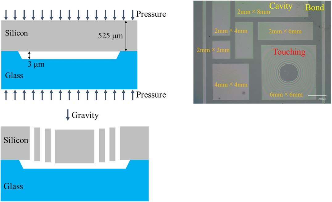
The MEMS structure consists of two layers as shown in Fig. 2. The first layer is a partially etched glass substrate of 700 μm thickness. The second layer is a silicon structure layer of 525 μm thickness. TSD is applied to this layer. The minimum gap of trenches is set to 25 μm. The glass layer is employed since it is advantageous in attaining low parasitic capacitances. The recess region in the glass is introduced to avoid touching between the movable structures and the glass substrate. To determine the recess depth, two cases are examined as shown in Fig. 3. Firstly, during the anodic bonding process, a pressure of 50 kPa is applied. As shown in Fig. 3(b) The touching is observed only in the size of 6 mm × 6 mm. If the cavity length is less than 4 mm, 3 μm depth is enough to avoid the touching. We determined the cavity length based on this observation. Secondly, after TSD, the movable parts should not touch the glass under gravity, as shown in Fig. 3(c). According to the simulations, the maximum deformation caused by gravity is 0.689 μm. Therefore, the recess depth is set to 3 μm to ensure sufficient margin. It should be mentioned that the deformation under gravity is larger than that by the pressure, since the silicon is etched by TSD in the former case.

Fig. 3. Deformation simulation: (a) cross-sectional model for anodic bonding, (b) cross-sectional view of fabricated chips under gravity, (c) experiment results of the deformation during the anodic bonding, and (d) summary of the gravity simulation results for all the chips on the same wafer.
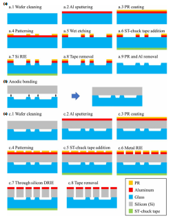
The MEMS process starts with a glass wafer used as the substrate. A recess region for movable structures is formed on the glass substrate. Firstly, an etching mask of 500 nm thick aluminum (Al) is sputtered onto the top of a glass wafer [Fig. 4(a.1–2)]. A photoresist (PR, PFI38A9) is coated onto the Al and the PR is pre-baked at 90 °C for 75 s [Fig. 4(a.3)]. In the development process, the developer NMD-W (2.38%) is used and the PR is post-baked at 110 °C for 5 min [Fig. 4(a.4)]. Then the exposed Al is etched with the mixed acid CMK-201 (25 °C, and 10 s to over-corrode) [Fig. 4(a.5)]. Since the glass is non-conductive, a conductive material needs to be formed on the backside to ensure electrostatic chucking during the plasma etching. For this purpose, we employed ACHILLES’ ST-chuck tape.19) After applying the ST-chuck tape to the bottom [Fig. 4(a.6)], the exposed glass is etched to a depth of 3 μm by reactive ion etching (RIE) [Fig. 4(a.7)]. As the etching gas, CHF3 is used. Finally, after removing the ST-chuck tape [Fig. 4(a.8)], the remaining Al is removed by a mixed acid CMK-201. The glass is then cleaned in piranha solution (H2SO4:H2O2 = 1:1, 120 °C, 10 min) [Fig. 4(a.9)].

Fig. 4. Fabrication process flow: (a) fabrication for a glass wafer, (b) Si wafer is anodically bonded to a partially etched glass wafer, and (c) fabrication for an anodic-bonded wafer.
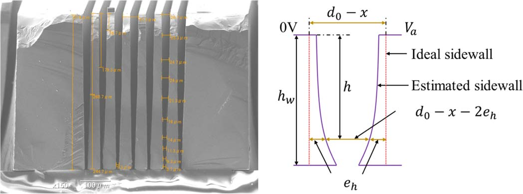
A non-vertical cross-sectional shape of trenches is shown in Fig. 9(a). This kind of taper has an impact on the device’s function. For example, it reduces the stroke of the movable components. Usually, a cross-sectional SEM is used to monitor the taper. This method, however, is destructive and cannot obtain taper distribution data over a wafer. In view of this, we developed a non-destructive method based on wafer level electrical measurements.

Fig. 9. Taper shape of trenches (a) SEM photo of actual taper, and (b) assumed taper shape.
5. Conclusions
In this paper, a fabrication process suitable for SOG-based low-resonant-frequency inertial MEMS sensors is presented. A thermal issue of TSD stemming from the low-resonantfrequency structure is prevented by enhancing the heat dissipation with two methods: introducing cooling time between the DRIE steps, and adopting a metal hard mask. These methods can be also applied to the fabrication process with a similar thermal issue. A blade dicing method suited for this device is also developed. To monitor the cross-sectional shape of the trench, a non-destructive method using CV data is shown.