Abstract: Two-dimensional silicon (silicene) and germanium (germanene) have attracted special attention from researchers in recent years. At the same time, highly oriented pyrolytic graphite (HOPG) and graphene are some of the promising substrates for growing silicene and germanene. However, to date, the processes occurring during the epitaxial growth of silicon and germanium on the surface of such substrates have been poorly studied. In this work, the epitaxial growth of silicon and germanium is studied directly during the process of the molecular beam epitaxy deposition of material onto the HOPG surface by reflection high-energy electron diffraction (RHEED). In addition, the obtained samples are studied by Raman spectroscopy and scanning electron microscopy. A wide range of deposition temperatures from 100 to 800 ◦C is considered and temperature intervals are determined for various growth modes of silicon and germanium on HOPG. Conditions for amorphous and polycrystalline growth are distinguished. Diffraction spots corresponding to the lattice constants of silicene and germanene are identified that may indicate the presence of areas of graphene-like 2D phases during epitaxial deposition of silicon and germanium onto the surface of highly oriented pyrolytic graphite.
1. Introduction
Two-dimensional materials, also known as two-dimensional crystals or 2D materials, are structures with a thickness of one or several atomic layers. The discovery of graphene, a monoatomic layer of carbon, in 2004 marked a significant breakthrough in the field of two-dimensional materials. Graphene is a unique two-dimensional allotrope of carbon with atoms arranged in a flat honeycomb lattice. Prior to the discovery of graphene, it was believed that extended two-dimensional crystals could only be stable at temperatures close to absolute zero. Unlike bulk materials, two-dimensional crystals have a high surface area to volume ratio, which affects their energy structure and electrical and optical properties.
The success in synthesizing graphene sparked interest in exploring other singleelement two-dimensional materials (transgraphenes) of groups 13–16 of the periodic table. Fabricating transgraphene materials is highly promising for the development of future nanodevices, offering increased efficiency and high speed. Consequently there has been a significant surge in both theoretical and experimental research focused on two-dimensional nanomaterials. Through the collaborative endeavors of scientists, numerous single-element two-dimensional materials have been successfully synthesized: borophene, gallenene, thallene, silicene, germanene, stanene, plumbene, phosphorene, arsenene, antimonene, bismuthene, selenene and tellurene. Extensive research is dedicated to exploring the exceptional properties of 2D materials and their potential in revolutionizing device design with novel operating principles. Particular attention is paid to graphene’s closest neighbors in group 14—silicene and germanene. An important advantage of these two novel materials is its direct compatibility with existing highly developed silicon technology.
Synthesizing transgraphene materials is an extremely challenging task in the present day. Graphene, a single layer of sp2 -hybridized carbon atoms, can be easily obtained by peeling off monolayers from graphite due to weak interlayer interaction. However, obtaining a monoatomic layer of silicon or germanium is much more difficult due to the sp3 -hybridization of the atoms and the strong covalent bonds. Consequently, exfoliation cannot be used to obtain silicene and germanene. As a result, the primary method for creating graphene-like materials is their epitaxial growth on lattice-matched substrates.
2. Materials and Methods
The growth studies presented in this work were carried out using the molecular beam epitaxy (MBE) on a Katun-100 installation. A preliminary vacuum was created by a vacuum station with a turbomolecular pump, and the presence of a degassing system for the epitaxy chamber, magnetic discharge pumps on each chamber, a sublimation pump and cryopanels allowed the pressure in the installation to be maintained at a level of <10−10 Torr during the epitaxial growth of structures. To evaporate Ge and Si materials, electron beam evaporators were used, which have a cooling system that ensures high purity of the material and stability of the evaporation rate of the material. To determine the deposition rate of Ge and Si material, there were two water-cooled quartz resonators with shutters. Shutters were also used to interrupt the flow of materials.
In this work, the epitaxial growth of germanium and silicon on commercially available HOPG wafers was studied. Before epitaxial growth, the top damaged layer of HOPG substrate was removed using acrylic tape. The foamed structure of the acrylic tape ensured the best uniform adhesion to the surface of the sample and uniform tearing of the top layer. Then, HOPG wafer was transferred to a high-vacuum chamber to maintain surface quality. In the growth chamber, it was thermally annealed at 1200 ℃. During annealing, the pressure in the chamber was maintained at a level of no more than 3 × 10⁻⁹ Torr. During the annealing process, the release of dissolved gases from the substrate, such as hydrogen, was recorded with the built-in mass spectrometer using the corresponding atomic mass peaks. After annealing, the temperature was dropped to growth temperatures; cooling occurred naturally. The temperature of HOPG substrate in the epitaxial chamber was controlled using an Optics 2.3 µm pyrometer.
3. Results
3.1. Epitaxial Growth of Si on HOPG
First of all, the original HOPG wafers were studied by reflection high-energy electron diffraction. HOPG sample consists of randomly oriented domains, all of which have the (0001) plane parallel to the surface. As a result, one can observe the diffraction spots from all the possible planes at the same time . Figure 1 shows the diffraction pattern from a clean HOPG surface.
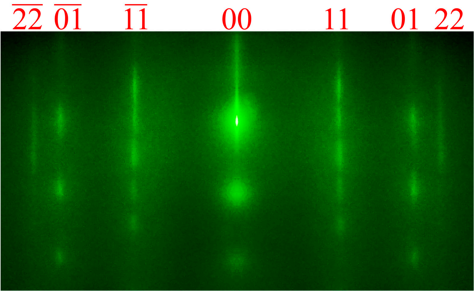
Figure 1. The characteristic diffraction pattern formed from a clean HOPG surface.
At 100 ℃, silicon grows amorphously on the HOPG surface (Figure S1a,b). The diffraction pattern after the deposition of 10 mL of Ge at 100 ℃ represents a homogeneous diffusion background (Figure 2b). When silicon is deposited onto HOPG at temperatures of 200–600 ℃ up to a thickness of 1 mL (Figure S1c–e), the diffraction pattern of the original HOPG does not change (Figure 2a). In this case, changes are not detected at any of the azimuthal angles when the substrate is rotated. This indicates that, up to this thickness, silicon follows the crystal structure of the substrate. When a larger number of silicon layers is deposited at 200–600 ℃, the growth pattern of Si on HOPG approaches polycrystalline growth. The diffraction pattern gradually loses intensity, but not as quickly as at low temperatures. Semicircles (Debye rings) begin to appear on a diffraction screen (Figure 2c). At a temperature of 650 ℃, silicon was deposited first to a thickness of 10 mL (Figure 2d) and then to 80 mL (Figure 2e). Up to an effective thickness of deposited silicon of 1 mL, no changes occurred in the diffraction pattern, but, with increasing coverage, a large number of additional reflections and semicircles began to appear, which persisted even at larger silicon thicknesses. An experiment was also carried out to anneal at 590 ℃ for 60 min a sample with 1 mL of silicon grown at 200 ℃ (Figure 2f). No changes in the diffraction pattern occurred during this process. From these results, it may be concluded that additional reflections in the diffraction pattern begin to appear only at temperatures above 650 ℃ after the deposition of 1 mL of Si.
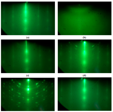
Figure 2. The characteristic diffraction pattern formed from (a) clean HOPG surface; (b) Si/HOPGsurface, growth temperature 100 °C, effective thickness of the deposited silicon 10 mL; (c) Si/HOPG400 “C, 10 mL; (d)Si/HOPG, 650 “C, 10 mL; (e) Si/HOPG, 650 “C, 80 mL; (f) Si/HOPG, 200°C,1 mIfollowed by annealing at 590 °C for 60 min.
Figure 3 shows the results of investigating the surface of Si/HOPG samples usingscanning electron microscopy,. Figure 3a shows an image of the surface of highly orientedpyrolytic graphite before silicon deposition. Smooth terraces are visible and a clear bound.ary between them (the edge of the step). A graphite flake is also partially visible, theexistence of which is possible on some areas of the surface. Figure 3b shows SEM image ofthe HOPG surface after the deposition of about 0.9 mL of silicon on HOPG. It can be seenthat silicon atoms coalesce as 2D islands on the surface of the HOPG terraces. oreover, alarge part of adatoms diffuse to the edges of the HOPG steps fmm contiguous regions ofthe lower adjacent terrace.
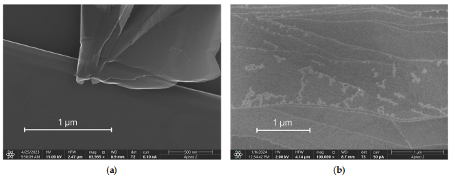
Figure 3. (a) SEM image of clean HOPG surface. (b) SEM image of the surface after deposition of 0.9 mL silicon on HOPG.
At low temperatures, germanium grew amorphously on HOPG. During the growthof Ge on HOPG at 170 °C, changes began to appear in the diffraction pattern after thedeposition of about 2 mL of germanium (Figure S2a). Then, within 8 mL, the formation ofDebye rings with weak point reflections of the 1/N type occurred (Figure 4b). The 1/Nreflections were located between the 00 and 11 lines of the original diffraction pattern forHOPG (Figure 4d) (details are in Section 4).
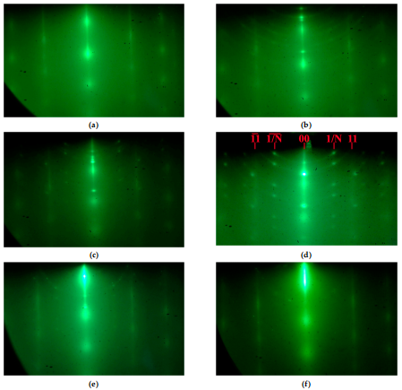
Figure 4. The characteristic diffraction pattern formed from (a) clean HOPG surface; (b) Ge/HOPGsurface, growth temperature 170 °C, effective thickness of deposited germanium 10 mL; (c) Ge/HOPG250 “C, 10 ml; (d) Ge/HOPG, 400 “C, 10 mL; (e) Ge/HOPG, 460 "C, 20 mL; (4 Ge/HOPG, 300 "C1 mL followed by annealing at 400 °C for 60 min.
Figure 5 shows the results of investigating the surface of Ge/HOPG samples usingscanning electron microscopy. Figure 5a shows the SEM image of the HOPG surfaceafter the deposition of about 0.9 mL of germanium. From this image, it can be seen thatgermanium preferentially assembles as elongated nanowires along the edges of the pristineHOPG steps. It should be noted that some of the edges of the terraces are completely filledwith germanium atoms (solid light lines), and some are only partially filled (dashed lightlines). In addition, there are a large number of regions containing 2D germanium layersthat fill the surface of the HOPG terraces in the form of individual 2D islands away fromthe edges of the steps. At later stages (several monolayers and more) germanium formschains of small 3D clusters along the HOPG edges (Figure 5b). The similar formation ofchains of 3D clusters has been previously observed by Shimonaka et al.. They have alsostudied, in detail, the features of Ge/HOPG deposition at higher germanium coverages(>10 mL of germanium).
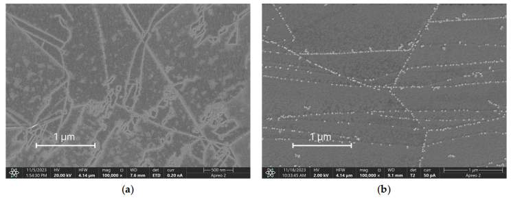
Figure 5. (a) SEM image of the surface after deposition of 0.9 mL germanium on HOPG. (b) SEM image of the surface after deposition of 10 mL germanium on HOPG.
Finally, Figure 8a shows the Raman spectra of the sample with 10 mL germanium on the surface of HOPG, grown at 400 ℃. Figure 8b compares the Raman spectra of a HOPG sample (blue curve) and the 10 mL Ge/HOPG sample (orange curve) near the point k = 300 cm−1 . Due to the small values of the signal, it was necessary to use a special technique for analyzing Raman spectra, developed by the authors. As a result, the presence of small peaks near 296, 300, and 304 cm−1 , corresponding to germanium, was established. This is consistent with the previous report on germanene, where Jung et al. revealed a Raman band at 296 cm−1 in a germanene sample. This line was also predicted theoretically by Kukucska et al.. The rest of the spectrum corresponded to the spectrum of the HOPG substrate. Low-frequency (7–200 cm−1 ) Raman spectra of the studied samples did not reveal any features (Figure S5).
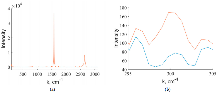
Figure 8. (a) Raman spectra of the 10 mL Ge/HOPG sample. (b) Raman spectra of the HOPG substrate (blue curve) and 10 mL Ge/HOPG sample (orange curve) near the point k = 300 cm−1 .
4. Discussion
From the results obtained, we can conclude that there are clearly defined temperatureintervals for the growth of silicon and germanium on HOPG. Within each interval, one oranother growth mechanism is realized. Thus, at temperatures close to room temperaturesilicon and germanium grow amorphously on the HOPG surface. When the temperatureincreases above 150°C, silicon and germanium begin to grow pseudomorphically, and, upto a thickness of 1 mL of the deposited material, their crystal structure repeats the structureof the substrate.
The dynamics of changes in the intensity of N reflections for different temperatures arenonlinear (Figure 9). Figure 9 shows the dependence of the moment of the appearance ofan additional 1/N reflection on the substrate temperature when Ge is deposited on HOPGThe inset to Figure 9 shows the dependence of the local intensity of the diffraction patternat the point of formation of the 1/N reflection on the effective thickness of the depositedgermanium on the HOPG surface (which is proportional to the grwth time). The Gegrowth rate for all curves was the same, equal to 0.02 mL/s. From this graph, it is clearthat, at temperatures below 450 C, the 1/N reflection appears at an effective thickness olthe deposited material of about 1 mL. Then, during the deposition of several monolayersthe intensity of this reflection reaches its maximum stationary value. The absolu te intensityvalue for all curves is apprximately the same, and, in the graph, the curves are shifted forclarity, The 1/N reflections persist for a sufficiently large number of deposited layers.
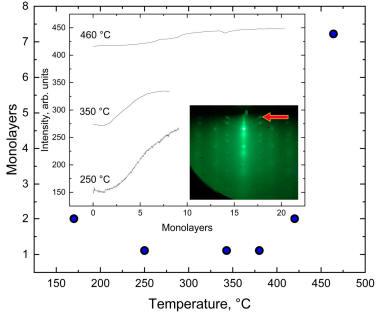
Figure 9. Moment of appearance of the 1/N reflection (shown by an arrow) in the diffraction patternduring the growth of Ge on HOPG at different deposition temperatures. Inset: dependence of thelocal intensity of the diffraction pattern at the point of formation of the 1/N reflection on the effectivethickness of the deposited Ge (the data are shifted vertically for clarity).
5. Conclusions
In this work, the epitaxial growth of silicon and germanium was studied directly in the process of material deposition onto the HOPG surface using reflection high-energy electron diffraction. In addition, the obtained samples were studied by scanning electron microscopy and Raman spectroscopy. A wide range of deposition temperatures from 100 to 800 ℃ was considered. Temperature intervals for various growth regimes of silicon and germanium on highly oriented pyrolytic graphite have been determined. It has been shown that, at temperatures close to room temperature, materials grow amorphously, and, at high temperatures, polycrystalline growth is observed. It has been established that the crystal structure of silicon and germanium within one monolayer repeats the structure of graphite. When the amount of deposited material increases to more than one monolayer in the intermediate temperature range (250–400 ℃ for germanium and above 650 ℃ for silicon), reflections of the 1/N type appear in the diffraction pattern (N(Si) = 1.56 and N(Ge) = 1.62). These values correspond to the lattice constants of silicene and germanene and may indicate the presence of areas of graphene-like 2D phases during the epitaxial deposition of silicon and germanium onto the surface of highly oriented pyrolytic graphite. The results obtained can be used to develop technology for the fabrication of silicene and germanene. In addition, the presented results will also be valid for the epitaxial growth of silicon and germanium layers on graphene, since it is single-layer graphite without underlying layers.