ABSTRACT
A single step growth approach for wafer-scale homogeneous cubic silicon carbide (3C-SiC) heteroepitaxy, using chemical vapour deposition (CVD), on a silicon (Si) substrate is demonstrated. Residual biaxial tensile strain causing a wafer bow is eliminated in the 3C-SiC epilayer via in-situ defects engineering and heteroepitaxy at reduced temperature. Thermal mismatch between the 3C-SiC epilayer and substrate is minimised by a substantial reduction of growth temperature, down to ~1000 ◦C. Heteroepitaxy of high quality, fully relaxed 3C-SiC epilayers with minimal wafer bow is demonstrated, made possible by careful process optimisation. Unusually very high growth rate of 3C-SiC of > 10 µm/hr is achieved. At the same time the epilayer is free from any other silicon carbide (SiC) polytype inclusions. Moreover, the reduced growth temperature unlocks the ability to deposit high quality 3C-SiC epilayers within traditional Si-based cold walled CVD reactors, enabling the growth of such thin films on unprecedently high volumes and wafer diameters up to 300 mm and above.
1. Introduction
Silicon carbide (SiC) is a wide bandgap compound semiconductor which shows high potential for the ongoing electrification of the world and creation of disruptive technologies in sensors, microelectromechanical systems (MEMS) and harsh environment electronics and optoelectronics. The next generation of power electronics can contribute in suppressing climate change by improving the efficiency of electric power conversion, which is applicable to a range of industries and social infrastructures. The high electric field breakdown and low switching losses of SiC make it ideal for high voltage and high frequency applications such as those found in electric vehicles. Also SiC possesses other excellent material properties at room-temperature such as high thermal conductivity (360 W m-1K-1), high hardness (9.3 Mohs hardness), and resistance to all wet and gaseous chemical etchants. It is not susceptible to damage from various forms of radiation as well. Semiconductor devices fabricated from SiC can operate at very high temperatures (>600 ◦C) and in harsh environments . These properties make it ideal for use in various applications beyond power electronics including microwave, harsh environment sensors, MEMS and biomedical devices. Also, relaxed cubic SiC, with a lattice constant of 0.436 nm, grown on a silicon (Si) substrate, is ideal virtual substrate for subsequent epitaxy of other scientifically and technologically important materials such as gallium nitride (GaN), aluminium nitride (AlN), boron nitride (BN),boron arsenide (BAs), Diamond and various 2D materials, including graphene, and thus allows their integration with Si. Successful device technology is greatly dependent on the wafer/substrate and epitaxial material quality.
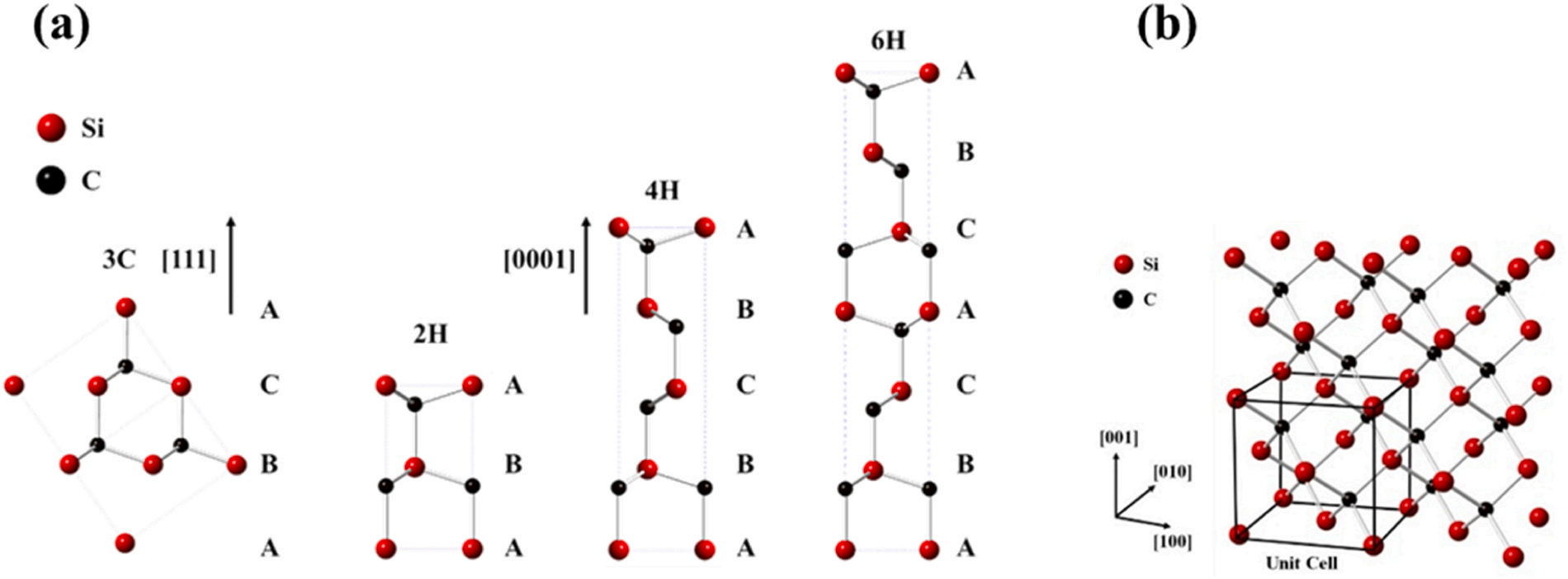
SiC exists in over 250 different crystalline forms called polytypes, see Fig. 1 . The hexagonal structured 4H-SiC dominates the SiC market due to the availability of crystalline wafers up to 150–200 mm diameter and well-developed homoepitaxial growth processes. While 4H-SiC is available in commercial applications, such as power devices and substrates for GaN and other III–V materials, 4H-SiC wafers are extremely expensive and subsequent homoepitaxy requires dedicated hot-walled chemical vapour deposition (CVD) reactors operated at very high temperatures over 1650 ◦C, which leads to high operating and maintenance costs. Nevertheless, 4H-SiC epilayers and substrates still contain various defects and polytypes inclusions.

Fig. 1. a) Unit cells of SiC polytypes: 3C-SiC, 2H-SiC, 4H-SiC and 6H-SiC (left to right). (b) Cubic crystal structure of 3C-SiC showing unit cell.
Initial growth processes for 3C-SiC were carried out at temperatures of ~1200 ◦C. To suppress the out-diffusion of Si and to create a seed layer for the subsequent epitaxy of 3C-SiC a silicon carbon alloy (Si1− xCx) buffer layer was deposited with approximately 1 % C composition. In contrast to well established carbonisation buffer, see Fig. 2a, which creates some graded Si1− xCx layer of poor quality and not even monocrystalline in the most cases, we used to innovation and introduced a defect free Si1− xCx alloy epilayer lattice matched to Si, which maintains the same crystallinity as Si substrate. As the growth process was further optimised, the deposition temperature was reduced to ~1000 ◦C at which point the out-diffusion of Si could be suppressed through optimising the C/Si ratio in the growth phase and as a result the Si1− xCx buffer layer was found to be unnecessary and a simplified process could be used, as shown in Fig. 2b. However, it could indeed be used as a seed layer for traditional high temperature 3C-SiC heteroepitaxy on Si.

Fig. 2. Heteroepitaxy of 3C-SiC on Si. (a) State of the art multi-steps 3C-SiC heteroepitaxy. (b) Novel reduced temperature heteroepitaxy growth process showing simplified steps and dramatically shorter processing time.
The grown 3C-SiC epi wafers were characterised using a range of techniques discussed below. The crystalline states of the grown 3C-SiC epilayers were verified using standard high resolution X-ray diffraction (HR-XRD) ω-2θ rocking curves and reciprocal space maps (RSMs) carried out on a Panalytical X’Pert MRD diffractometer with CuKα1 radiation. HR-XRD can quantify the crystal quality of the epilayer and assess whether the films are monocrystalline, polycrystalline, amorphous and under significant levels of tilt or residual strain. Atomic Force Microscopy (AFM) was performed on as grown samples to determine the surface morphology and roughness using a Bruker Icon AFM operating in Scan assist mode. Cross-sectional transmission electron microscopy (X-TEM) is one of the most effective techniques to assess the crystallinity and morphology of 3C-SiC epilayers. When preparing electron transparent samples for X-TEM, traditional mechanical grinding and Ar beam milling are effective on 3C-SiC epilayers below ~1 µm thick and more complex extraction techniques such as focussed ion-beam (FIB) can be avoided. X-TEM samples were prepared through the use of SiC grinding pads and Ar ion polishing and X-TEM micrographs were obtained on a JEOL 2100 TEM. Thickness uniformity measurements were performed on a Bruker Vertex V70 FTIR and wafer bow measurements were obtained on a Bruker DektakXT stylus profiler.
3. Results and discussion
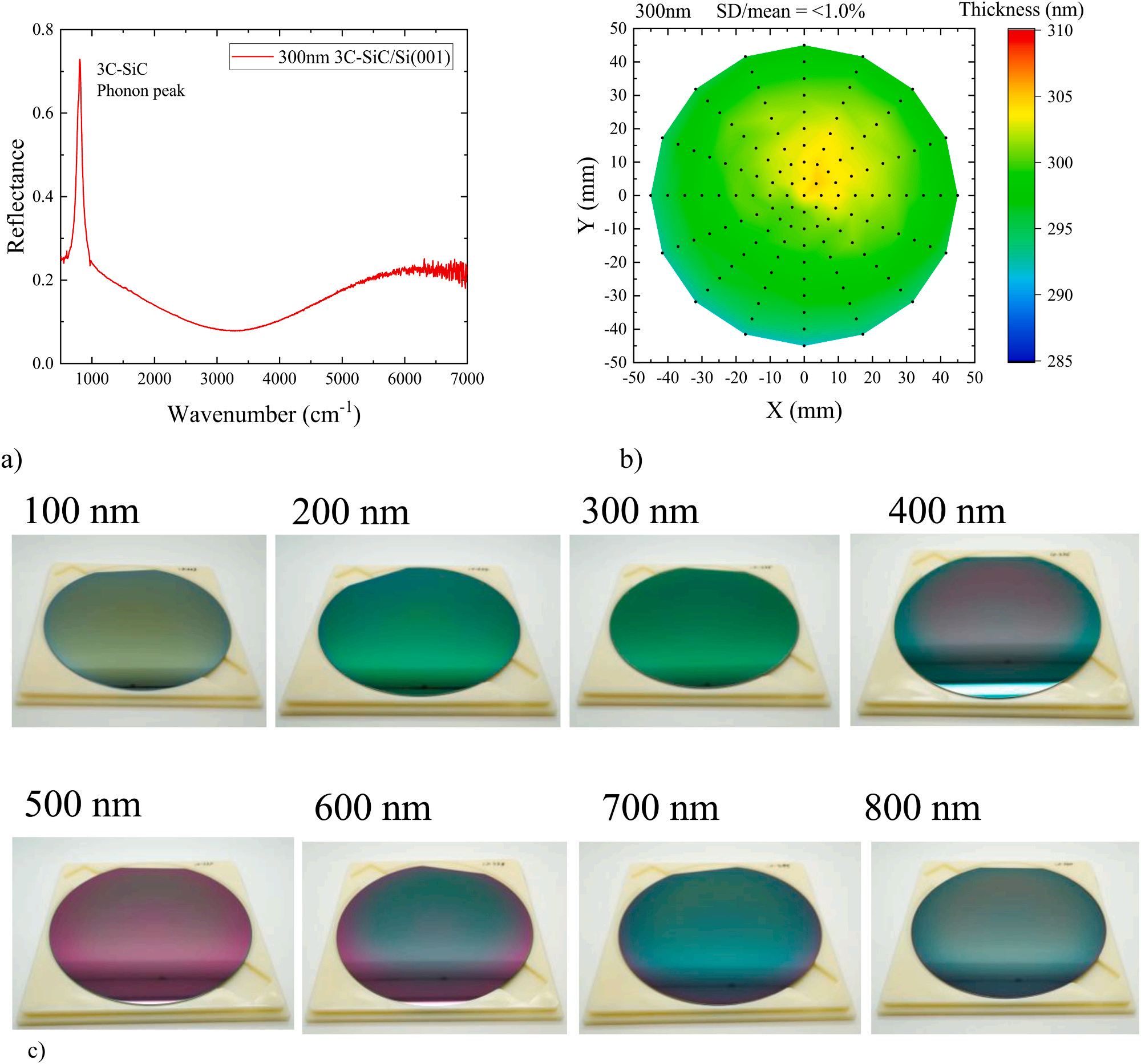
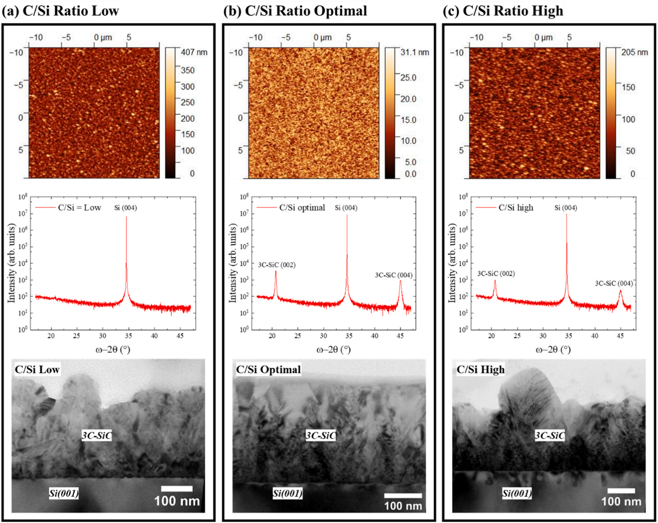
After the selection of appropriate precursors, the C/Si ratio must be adjusted in order to grow a high quality 3C-SiC compound epilayer, but not a Si1− xCx alloy [19] or SiC compound with high density of interstitial Si or C defects. Correct C to Si ratio is absolutely essential to obtain SiC compound of any polytype including 3C-SiC. Thermal decomposition of any Si or C precursor depends on the bonding energy of a particular precursor molecule and therefore could create more or less Si or C atoms emerging on the substrate’s surface. A 3C-SiC epilayer grown under optimum growth conditions exhibits the lowest surface roughness and the highest crystal quality. Characterisation results from samples growth with reduced, optimal and increased C/Si ratios can be seen in Fig. 3. Non-optimal growth conditions produce very high surface roughness implying poor island growth mechanisms with high levels of interstitials, however, at optimal C/Si ratio a very low RMS of ~3 nm can be achieved, which results in a mirror-like surface of the 3C-SiC/Si(001) epi wafer, see Fig. 7.

Fig. 7. Wafer uniformity. (a) FTIR reflectance spectrum for a 300 nm thick 3C-SiC epilayer. (b). Wafer uniformity of a 100 mm 3C-SiC epi wafer showing uniformity of < 1.0 % across 90 % of the wafer diameter. (c) Epi wafers of various 3C-SiC epilayer thickness exhibits superior uniformity visible due to colour variation of wide band gap 3C-SiC epilayer grown on Si.
When the C/Si ratio is low, no 3C-SiC epilayer Bragg peaks at (002) and (004) reflections in ω-2Θ scan are visible implying that the grown film is polycrystalline or amorphous and a sufficient level of C is required to initiate monocrystalline epitaxy. Growth of 3C-SiC grown using an optimal C/Si ratio resulted in the strongest Bragg peaks at (002) and (004) reflections with the lowest FWHM suggesting highly crystalline 3C-SiC. No polycrystalline peaks are observed in the ω-2Θ scan. When the C/Si ratio is higher than optimal, the 3C-SiC remains crystalline with only a slight reduction in peak intensities and broadening of FWHMs suggesting an excess of C in the growth phase has only a minor impact on crystal quality. Therefore, the structure of the 3C-SiC thin films varies dramatically with C/Si ratio and characterisation results obtained with AFM, XRD and XTEM, shown in Fig. 3, correlates very well. When the C/Si ratio is non-optimal, poor crystallinity is observed in the films and extremely rough surface morphology implies 3D island growth modes. For low C/Si ratio the 3C-SiC thin film is polycrystalline. For optimal C/Si ratio, the epilayer is observed to be crystalline throughout, with smooth surface, abrupt 3C-SiC epilayer and the Si(001) substrate interface. Also, voids formation in the Si substrate is completely eliminated, even without the inclusion of a buffer layer or carbonisation. More details of the C/Si ratio impact on the materials properties of the 3C-SiC thin films will be published elsewhere.

Fig. 3. Influence of C/Si ratio on the properties of 3C-SiC epilayers showing surface morphology with AFM maps, crystallinity with HR-XRD coupled scans and structure and defect formation in X-TEM micrographs for low, optimal and high C/Si ratios.
Almost full strain relaxation, or in other words very small residual tensile strain, i.e. < 0.1 %, occurs within the 3C-SiC epilayer, grown with optimum C/Si ratio, which suppresses the wafer bow. As an example, Fig. 6 shows the wafer bow of a 100 mm diameter 3C-SiC/Si (001) epi wafer with 300 nm 3C-SiC epilayer. Only very small warp can be observed in the 3C-SiC/Si epi wafer which is below < 20 µm at its maximum. This level of wafer warp is expected in Si substrates and hence the addition of the low temperature grown 3C-SiC epilayer has had little to no effect on the bow of the wafer. The typical acceptable wafer bow for a wafer to be processed for subsequent semiconductor device fabrication by, for an example, a lithography equipment is up to ~250 µm and for high resolution lithography processes even less bow, of < 50 µm, can be tolerated. The 3C-SiC epi wafer shown above is well below this limit and is therefore suitable for all subsequent processing steps. It is interesting to note, that the reduced temperature process also opens the possibility to grow 3C-SiC on much thinner Si wafers, i.e. ~200 µm, which are essential for MEMS, sensors and photovoltaic devices applications or others where the thin Si wafer is essential or Si wafer has to be etched partially or completely.

Fig. 6. Wafer Bow. (a) 3D map of wafer distortion across a 300 nm thick 3C-SiC epilayer grown on a standard 525 µm thick 100 mm diameter Si(001) substrate. (b) Line scan showing wafer bow across the 300 nm 3C-SiC/Si(001) diameter. (c) The resulting 3C-SiC epi wafer is completely flat and no bow is observable optically. The typical acceptable wafer bow for a wafer to be processed for subsequent semiconductor device fabrication by, for an example, a lithography equipment is up to ~250 µm and for high resolution lithography processes even less bow can be tolerated (<50 µm).
The proposed epitaxial process is also transferable to other Si substrate orientations including Si(111), which offers a template for hexagonal materials such as AlN and GaN. 3C-SiC/Si(111) virtual substrates provide a low-cost and large diameter alternative to 4H-SiC substrates for GaN devices, including RF communications, power devices and LEDs while still offering the same low lattice mismatch of just 3.4 %, low diffusivity of impurities and high thermal conductivity. Finally, the 3CSiC/Si virtual substrate can be used for heteroepitaxy of Graphene and other 2D materials.
4. Conclusions
In conclusion, the novel approach reported here has created a technology, which allows not only wafer scale homogeneous 3C-SiC heteroepitaxy on on-axis Si(001) wafer, but also beyond state of the art 3CSiC epitaxial material quality. Moreover, the process is much simpler, faster, cheaper, substantially less energy consuming and consists of just a single growth step comparing to traditional multi-steps. High quality 3CSiC epilayers can be grown at low temperatures down to ~1000 ◦C without the requirement for carbonisation or other buffer layers. High growth rates of above 10 µm/hr are achievable, which would enable the growth of very thin and very thick epilayers from 10’s nm up to 10’s µm covering a wide range of applications. High crystallinity, low surface roughness, minimal wafer bow and excellent uniformity both across each wafer and from run to run is achieved with this technique. Crucially the process can be run in a Si-based cold-walled CVD system. The process is comparable to standard Si epitaxy and offers 3C-SiC growth at a similar cost point and scale. Various other technologies are also unlocked within such reactors and reduced growth temperatures, including selective epitaxy on SiO2 patterned substrates, blanket growth on SOI wafers and integration with other technologically important Group IV semiconductors.
下一篇: 高取向热解石墨上硅和锗的外延生长