Abstract.
Decapsulation is the process of opening the polymer layer covering the die. The purpose of decapsulation on IC is to facilitate checks on the quality of the die. The method carried out in this study uses the method of dripping H2SO4 on the IC surface. The variables to be examined in this study are variations in the use of H2SO4 volume and H2SO4 temperature. The volume variation used consists of 0.1130 ml (10 drops), 0.1356 ml (12 drops) and 0.1582 ml (14 drops). While the temperature variation used in this study consisted of 165 °C, 170 °C and 175 °C. The results showed that all samples is not completed decapsulation process. Some samples (B, C, E, F, H, and I) is partial decapsulation while other sample is not open die at all. Moreover, Sample C exhibits the greatest thickness reduction among all the samples under examination, and the die is distinctly visible.
1 Introduction
Integrated circuit (IC) packaging is the last step in the manufacturing process of an electronic device. The system board's external circuitry and the chip are connected electrically by the IC packaging, which serves this function as its primary function. Device will be put through a functional test after the packaging stage. IC packaging fills the gap between production of semiconductors and implementing the finished product. Wire bonding, often referred to as sequential bonding, is a common connecting technique for packages that uses metallic wires to link IC chips and substrates. To be more exact, local heat produced by ultrasonic vibrations is used to establish these first-level junctions using Cu or Au wires that span between the substrate pads and die.. Nevertheless, because of its atomic structure and physical characteristics, there are certain issues regarding the reliability of copper wire. In the bond pad, copper and aluminum generate intermetallic compounds. Copper corrodes when it is exposed to moisture and the mold compound's chlorine. Additionally, due to copper's high coefficient of thermal expansion (CTE) discrepancy with molding material, cracks appear at the bond pad interface or wire neck. Phenolic hardeners, epoxy resins, catalysts, silicas, pigments, and mold release agents are the main components of the molding compound, which is a composite material. The capability to reliably decapsulate these devices is required in order to perform quality control tests on microelectronics, which may necessitate further failure studies and subsequent circuit changes. In the failure analysis process, the fundamental and crucial function of a wire bonding device's decapsulation is to produce an electrical reliable device with its die disclosed for analytical work. A key factor in the failure of wire bond packages is the decapsulation process. Maintaining the wires in their packaging without causing any damage is essential while removing polymer encapsulants like epoxy molding compounds (EMC). When a device is decapsulated, the whole mold compound should be removed from the desired location without affecting the electrical properties of the device. There are three methods for package decapsulation that are frequently used: wet chemical etching, laser ablation, and plasma etching. From the previous study of Murali S, it shows that the epoxy molded packages can be decapped without affecting the copper wire bonds and their interfaces by using a mixture of fuming nitric acid and 96% concentrated sulfuric acid. The use of variation temperatures in a range of 90-230 °C where the results are good for some various temperature such as in a 150 and 160 °C. Similar with the experiment of Ng S, Cu wire-bonded packages can be extracted via wet chemical etching. The findings of these tests demonstrate that it is possible to create successful Cu wire-bonded devices, which means that further failure analysis phases involving complete device functionality can be carried out without any restrictions. Due to its efficiency and speed, wet chemical etching has been regarded as the best method. The wet approach is performed using nitric acid (HNO3), sulphuric acid (H2SO4), or a mixture of both of those acids. A significant factor that can result in either under or over-etching is the acid volume used to remove the protective shell of the IC electronic device. Also, decapping is more effective at higher acid temperatures, although fine wire, particularly copper, may corrode. In this paper we studied the effect between various temperature and acid volume in a decapsulation process of the Integrated Circuit (IC) packaging device. The manual wet method is used in this study. Furthermore, identification and analysis of the IC are presented after decapsulation process has been completed.
2. Method
The above activities can be described with the following explanation: A. IC Preparation The start of the activity is to prepare the IC that will be used as an experimental sample. The IC used was 9 samples. B. Measurement of IC thickness Before carrying out decapsulation process, the thickness of each IC is measured (in millimeters) using a digital caliper. Measurements were carried out 25 times for each IC, it was done to obtain variations in accurate IC thickness measurement results. C. Observation surface of IC The next step, looking at the shape of each IC using a Keyence digital microscope. Keyence is a microscope with an all-in-one system (viewing-recording-measuring). This machine can observe uneven surfaces and 3D objects, it has a depth of focus up to 20 times greater. Keyence designs its own lenses, cameras and graphics engines, so that observations can be made with an optimal balance of brightness and clarity. D. Decapsulation process The volume variation used consists of 0.1130 ml (10 drops), 0.1356 ml (12 drops) and 0.1582 ml (14 drops). While the temperature variation used in this study consisted of 165 °C, 170 ° C and 175 °C.

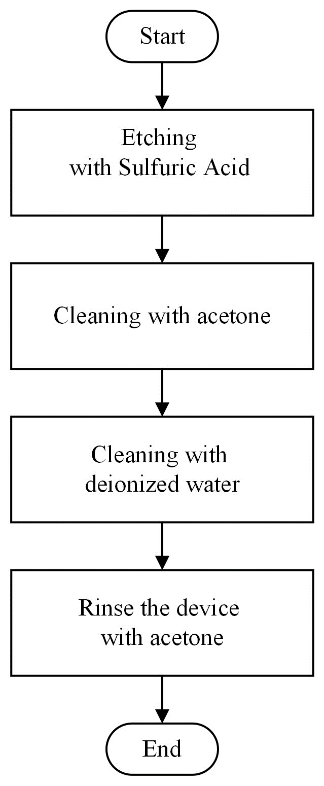
Fig 1. Flowchart of the experimental design
2.2 Description of Decapsulation Procedure
The procedure above can be described with the following explanation: A. Etching with Sulfuric Acid The IC is placed on a hotplate which is based on a porcelain cup, the function of the cup is to react substances at high temperatures, then wait until the temperature on the IC reaches the desired temperature. Furthermore, drop sulfuric acid on the IC according to the desired dose as in Table 1. The epoxy molding compound is dissolved using 100% concentrated sulfuric acid. If the plastic layer on the IC packaging has peeled off, lift the IC immediately from the hotplate, so that the wire is not broken. B. Cleaning IC The IC is cleaned using acetone to see the condition of the IC. After cleaning the IC using acetone, then the IC is cleaned again with deionized water to see the condition of the IC. C. Rinse the device with acetone The function of the rinse is to clean up the remaining abrasive layers of the decapsulated mold compound. D. Thickness measurement After the IC decapsulation process is successful, then take measurements again on the IC to check the thickness of the IC using a digital caliper. This activity was carried out to see the difference in thickness of the IC before and after the decapsulation process. E. Observation IC after decapsulation View and re-observe the shape of the IC that has gone through the decapsulation process using a Keyence digital microscope. This activity was carried out to see the difference in IC shape before and after decapsulation process.F. Analysis of Data Collect all data from observations and measurements, and then carry out data analysis. It aims to determine the differences in thickness and shape of IC before and after IC decapsulation, the influence of acid temperature and acid volume and concentration of sulfuric acid. The decapsulation process in the research can be seen in Figure 2.

Fig 2. Decapsulation Procedure
3 Result and Discussion
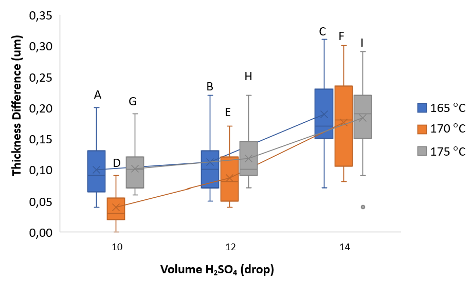
The effect of volume variation on IC thickness for all samples can be shown in Figure 3.

Fig. 3 Box Plot the effect of H2SO4 volume variation on the thickness of all samples
Based on Figure 3, the variation in the volume of H2SO4 dripped on the IC surface affects the thickness of the IC. The highest thickness difference belonged to the sample group given 14 drops of H2SO4. In general, an increase in the volume of H2SO4 on the IC surface has a linear relationship with the reduction in IC thickness.
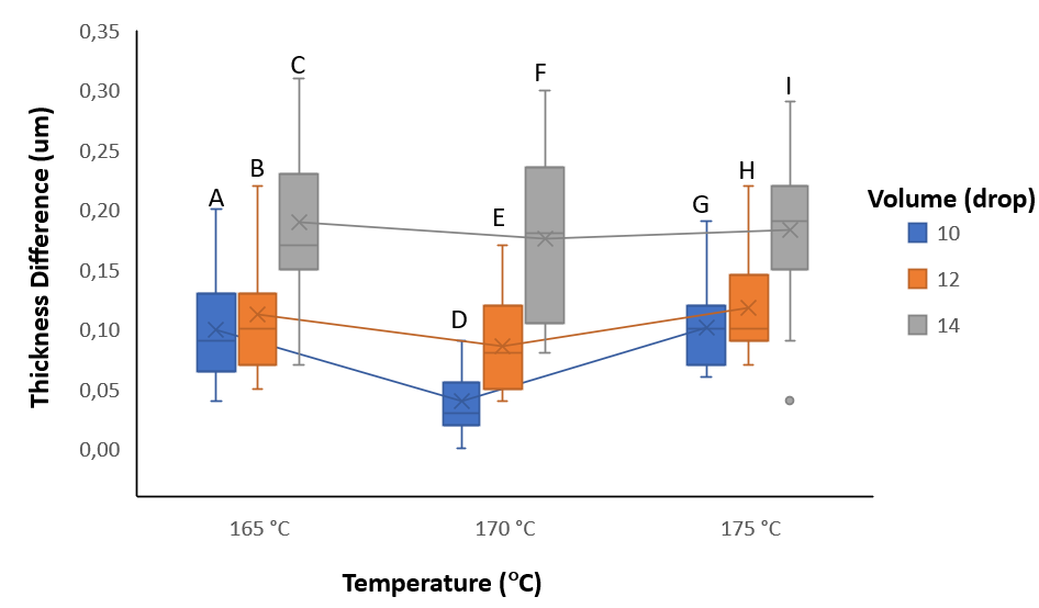
The same data, data processing was carried out to see the effect of temperature on all samples (Figure 4).

Fig. 4 Box Plot the effect of temperature variations on the thickness of all samples
Based on Figure 4, the temperature variation of H2SO4 applied to the IC surface affects the thickness of the IC. Overall, the sample group given H2SO4 with a temperature of 170 °C showed a lower IC thickness difference compared to other temperature variations. As for the sample group given H2SO4 with temperatures of 165 °C and 175 °C relatively has the same pattern for IC thickness reduction.
4 Conclusion
Decapsulation is the technique that can be used to analyse failures in ICs. When the complete decapsulation process occurs on the IC surface, the condition of the Die covered with polymer material can be analysed for its functionality. Based on the research, complete decapsulation has not occurred in all samples. Decapsulation is only partially open in some samples (B, C, E, F, H, and I). While other samples (A,D,G) have no open surface at all. The die is more clearly visible on sample C with the temperature used and the volume used is 165 °C, 14 drop respectively. In addition, sample C has the highest thickness reduction of all samples under test.
上一篇: 碳纳米管集成电路技术路线图及技术挑战
下一篇: 低温下在硅晶片上进行单步碳化硅异质外延