Abstract
As the manufacturing process of silicon-based integrated circuits (ICs) approaches its physical limit, the quantum effect of silicon-based field-effect transistors (FETs) has become increasingly evident. And the burgeoning carbon-based semiconductor technology has become one of the most disruptive technologies in the post-Moore era. As one-dimensional nanomaterials, carbon nanotubes (CNTs) are far superior to silicon at the same technology nodes of FETs because of their excellent electrical transport and scaling properties, rendering them the most competitive material in the next-generation ICs technology. However, certain challenges impede the industrialization of CNTs, particularly in terms of material preparation, which significantly hinders the development of CNT-based ICs. Focusing on CNT-based ICs technology, this review summarizes its main technical status, development trends, existing challenges, and future development directions.
1. Introduction
Over the past half-century, the chip industry has progressed significantly due to Moore’s law (the integration of chips doubling every 18 months), which has profoundly changed the pattern of people’s lives and industries. During this transformation, the rapid iteration of new technologies constantly refreshes the technical nodes of Si-based chips, thereby surpassing Moore’s limits in several cases. However, in the second decade of the 21st century, the development speed of the chip process decreased significantly, mainly because the scale of Si-based field-effect transistors (FETs) approached the physical limitations. Currently, benefiting from advanced technologies such as extreme ultraviolet lithography, the mature manufacturing process has entered the 4 nm technology node, and the industry is evolving to the 3 nm or even 1 nm node. Each step forward incurs significant costs and requires a longer time to understand the core technologies. Moreover, merely relying on enhancing manufacturing techniques to improve the performance of Si-based chips cannot fully satisfy the current demands.
According to the latest International Technology Roadmap of Semiconductor (ITRS) , the short-channel effect becomes increasingly concerning as the technology node approaches its physical limits, as it results in the failure of microelectronic devices to follow the principles of traditional semiconductor physics. Hence, the potential of Si-based chips is almost exhausted, and Moore’s law is no longer applicable. New materials and manufacturing methods are internationally recognized methods for fundamentally solving problems associated with chip performance, whereas carbonbased semiconductors are considered disruptive technologies in the post-Moore era.
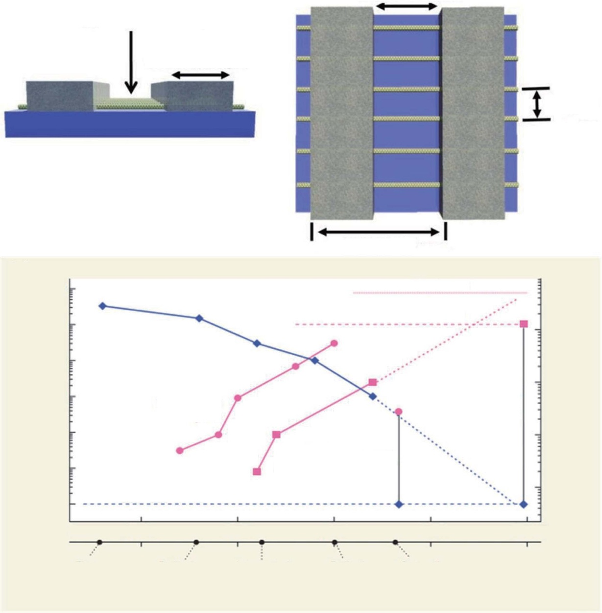
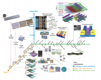
Currently, CNT-based transistors are expected to approach the performance limit determined by the laws of quantum mechanics and thermodynamics defined through continuous technical research, which demonstrates the significant potential of CNT electronics. According to researchers at the IBM Watson Research Center, the process for manufacturing high-performance ICs comprising CNTs will be different from the current lithography process of Si (figure 2). A purification above 99.9999% of semiconductor CNTs (s-CNTs) must be strictly controlled, and CNTs in channels should be densely aligned with a density exceeding 125 tubes·µm−1 such that the performance of CNT-based transistors can exceed that of Si (figure 3). However, according to the latest international reports, significant challenges remain that hinder the development of CNT chips. Therefore, this review summarizes the recent progress of s-CNT purification, the regular assembly and cross-scale manufacturing of ICs, and the prospects for the manufacturing technology of CNT-based ICs.

Figure 2. Schematic illustration of a CNT FET modeled for 5 nm technology node. (a) Side view of a device showing CNTs between the source and drain. The gate will be located either around each CNT or on top of the array (omitted herein for clarity). (b) Top view of a device showing multiple CNTs between the contacts. The key dimensions are the gate pitch and CNT pitch. (a) and (b) Reprinted with permission from. Copyright (2014) American Chemical Society. (c) Progress of CNT transistor technology. Reproduced from, with permission from Springer Nature.

Figure 3. Purify-align-integration manufacturing of CNT-based integrated circuits (ICs). Purify: extracting semiconductor CNTs from mixed CNTs; align: arranging disordered CNTs into aligned arrays; integration: manufacturing of CNT-based transistor arrays.
2. Preparation of s-CNTs with high purity and high yield
The intrinsic properties of CNTs are affected significantly by their chirality. Structurally, CNTs can be viewed as a single sheet of graphite seamlessly curved along a certain direction to form a tubular structure. And the chiral coefficient (n, m) characterizes the wrapping direction and determines the size of the wrapping angle. Due to the fact that different electronic properties exhibited by CNTs strongly depend on the wrapping angle, researchers typically use chiral coefficients to characterize certain types of CNTs. Specifically, when n = m, CNTs have bands crossing the Fermi level and are therefore metallic. And these particular CNTs are called armchair tubes. The remaining types exhibit two possibilities. When n–m = 3 l (where l is an integer), tubes are also expected to be metallic. In the case n–m = 3 l, tubes are predicted to be semiconducting.
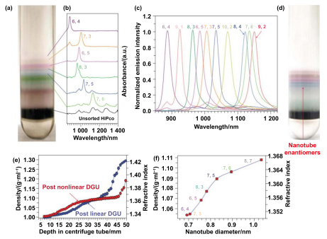
Surfactants such as sodium dodecyl sulfate (SDS) and sodium dodecyl benzene sulfonate (SDBS) can effectively disperse CNTs in aqueous solution. Notably, surfactants exhibit extremely low selectivity for different types of CNTs. After suspension formation, density gradient ultracentrifugation (DGU) or column chromatography is generally performed to further purify CNTs. Arnold et al first used the DGU method to classify CNTs , where single-stranded DNA and iodine octanol were used as the surfactant and density gradient medium, respectively. Under a long duration of high-speed centrifugation, the CNTs were layered in the solution based on their diameters. This study achieved a high purification efficiency for small-diameter s-CNTs, and the chiral types were (6,5), (9,1), and (8,3). Subsequently, Weisman’s group improved the DGU method using a customized S-shaped gradient centrifuge tube , as shown in figure 4. This centrifuge tube had a very shallow gradient and was nonlinear. Under the action of an ultrahigh centrifugal force, even CNTs with insignificant chirality differences can be separated, thus significantly improving the resolution accuracy of the chirality. Using this method, researchers extracted up to 10 types of chiral s-CNTs from HiPCo carbon tubes, with diameters ranging from 0.7 nm to 1.1 nm and the highest purity of 88%.

Figure 4. Sorting of single-walled carbon nanotubes by nonlinear density-gradient ultracentrifugation (DGU). (a) Distinct colored bands are layers enriched in different CNT species. (b) Near-infrared absorbance spectra of the marked colored layers. (c) Photoluminescence spectra of 10 separated fractions. (d) Centrifuge tube showing resolved pairs of enantiomer bands sorted from HiPco CNTs via nonlinear DGU using a single surfactant (sodium cholate). (e) Density profiles of DGU medium for linear and nonlinear initial gradients. (f) Densities of sodium cholate-suspended CNT species as a function of CNT diameter. Reproduced from, with permission from Springer Nature.
Subsequently, Liu et al improved the efficiency of PCz using a multiple dispersion and sorting process. Considering that dispersion effects depend on solvent selection, this method uses vacuum filtration to transfer the solvent environment during purification. The assembly of CNTs and polymers was successively subjected to ultrasonic tip and high-speed centrifugation in toluene, tetrahydrofuran, and trichloroethane. Finally, s-CNTs with a purity exceeding 99.9999% were obtained, which satisfied the level required for chip manufacturing.
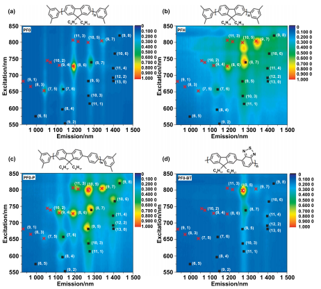
Nish et al used conjugated polymers for the separation of metallic/semiconductor CNTs in 2007. Conjugated molecules such as polyfluorene, polycarbazole, and polythiophene can spirally wrap the outer walls of s-CNTs to form a stable assembly in the solvent. They exhibit ultrahigh selectivity for specific types of CNTs depending on their side chains and bodies (figure 5).

Figure 5. Highly selective dispersion of single-walled carbon nanotubes with aromatic polymers and photoluminescence excitation maps of various polymer-CNT samples in toluene solutions. (a) Maps for polymers PFO, (b) PFH, (c) PFO-P, and (d) PFO-BT. Reproduced from [50], with permission from Springer Nature.
3. Large-scale and regular assembly techniques of CNT arrays
To fabricate CNT-based ICs, disordered CNTs must be rearranged to be placed into aligned arrays on a wafer scale, with the density of the CNTs satisfying certain requirements. IBM researchers proposed densifying CNTs to more than 125 tubes·µm−1 and controlling their inter-tube pitch to 5 ∼ 10 nm to achieve state performances better than those of Si-based transistors.
In earlier studies, researchers mainly modified the substrate, particularly the oxidation medium layer related to the manufacturing of electronic devices. Liu et al formed hydrophilichydrophobic functional layers arranged alternately on a silicon dioxide (SiO2) substrate using -CH3 and -NH2 terminal groups. When the substrate was immersed in a DMF solution containing CNTs, the nanotubes deposited spontaneously on the hydrophilic surface via interactions. Meanwhile, Bardecker et al modified the substrate surface of Al2O3 and HfO2 with alkylphosphonic acids. They realized the selective deposition of CNTs via micro-imprinting and lithography. However, an ideal alignment of nanotubes was not achieved in these earlier studies owing to the limitations of the patterning resolution.
4. Manufacturing technology of CNT-based ICs
To improve the purity of s-CNTs and the quality of alignment arrays, the semiconductor device manufacturing technique and basic conditions allow the multiscale fabrication of CNT-based ICs, which is beneficial to the manufacture of high-performance CNT-based ICs that are comparable to or better than Si-based chips. The fabrication of CNT-based ICs is based on regular arrays of s-CNTs with a large area, an ultrahigh density, and high purity
5. Conclusion and prospect
Currently, the development of CNT-based chip manufacturing technology has indicated significant achievements; however, main obstacles must be broken through before s-CNTs can be industrialized. To surpass the performance of Si-based chips, CNT-based chip technology should be further developed as follows: (1) the preparation of high-quality and high-yield s-CNTs. In this respect, the solution method is preferred. The purity of s-CNTs prepared using the polymer purification method exceeds the 99.999 9% standard required for large-scale ICs. Moreover, for the same technology node, the state performance of CNT-based FETs surpasses that of Sibased FETs. However, this ultrahigh purity was achieved at the expense of production yield. Although an increase in the number of process steps improves the quality, it also significantly increases the manufacturing cost, which does not provide a competitive advantage. In the future, the development of CNTbased technology should be low cost. (2) Reliable large-scale fabrication of aligned CNT arrays. High performance CNTbased transistors impose strict requirements on the arrangement of CNTs in the channel, that is, to achieve a high density (>125 tube·µm−1 ) while ensuring reasonable spacing (5 nm). To manufacture ICs, hundreds of billions of CNTs must be arranged in a highly ordered manner on a macro scale. Existing methods of DNA and pull-up assemblies satisfy these requirements; however, the repeatability and stability must be improved. (3) Establishment of technological process standards for CNT-based ICs. We think that this section is based on overcoming material challenges and forming a uniform technological process to achieve device homogeneity and stability preparation. Currently, the manufacturing process for highly 16Int. J. Extrem. Manuf. 6 (2024) 032004 Topical Review integrated CNT FETs is not consistent in many works, especially the unique cleaning, CMOS doping, and electrode contact process steps of CNTs. In the future, new technologies need to be broken through to apply to smaller CNT FET nodes, such as CNT-BNNT heterostructure nanotube and high k gate dielectric materials, to solve the contact and gate control issues of extremely scaled devices.