Y-stabilized ZrO2 (YSZ) as a promising single-crystal wafer material for the epitaxial growth of transition metal dichalcogenides applicable for both physical (PVD) and chemical vapor deposition (CVD) processes is used. MoS2 layers grown on YSZ (111) exhibit sixfold symmetry and in-plane epitaxial relationship with the wafer of (1010) MoS2 || (211) YSZ. The PVD-grown submonolayer thin films show nucleation of MoS2 islands with a lateral size of up to 100 nm and a preferential alignment along the substrate step edges. The layers exhibit a strong photoluminescence yield as expected for the 2H-phase of MoS2 in a single monolayer limit. The CVD-grown samples are composed of triangular islands of several micrometers in size in the presence of antiparallel domains. The results represent a promising route toward fabrication of wafer-scale single-crystalline transition metal dichalcogenide layers with a tunable layer thickness on commercially available wafers.
Transition metal dichalcogenides (TMDCs) are considered aspromising next-generation optoelectronic materials, owingtotheir intriguing physical properties appearing as a result of anintrinsically layered structure, specifc crystal symmetry, anddistinctly different optoelectronic properties of a large varietyof polytypes.To fully understand and explore the potentiaof TMDCs, single-crystalline wafer.scale flms with tuneablematerial composition, layer thickness, and crystalline excellencecomparable to,or even exceeding that of currently availablebulk crystals, are needed.However, synthesis of the flms,satisfying these requirements, remains very challengingDespite van der Waals nature of the materials, growing them on available non.van der Waals wafersleads to a strong nuclei-wafer interaction,predefining structural imperfection of thedeposited layers. The choice of suitablesubstrates for the epitaxialgrowth ofTMDCs is limited not only by purelycrystallographic considerations, but alsowafer resistance against melting, decompo.sition, and chemical reactions with chalco.gen atoms at elevated temperatures. Theseconditions are required for the most widelyused fabrication technigues, includingphysicaldeposition(PVD)andvaporchemicaldeposition(CvD). Thevaporcommonly used basal plane of sapphireis thermally and chemically stable andwithstands even the harsh environmentofthe CVD process.
2. Results and Discussion
ZrO2 can be stabilized by Y as a face-centered-cubic fluorite structure with a lattice parameter depending on the Y-molar fraction. The material is generally known as a substrate for In2O3-based bixbyite compounds. A closely packed YSZ (111) cubic substrate (a = 5.147 Å, Crystec GmbH) with a nominal Y doping level of 9 mol%) exhibits an in-plane lattice spacing along the [110] direction of aYSZ 110 = 3.639 Å. This coincides with the in-plane lattice parameter aMoS2 of 2H-MoS2 with a lattice mismatch of about –13.1%. At first, we address the PVD growth of multilayer and single-monolayer (ML) films.
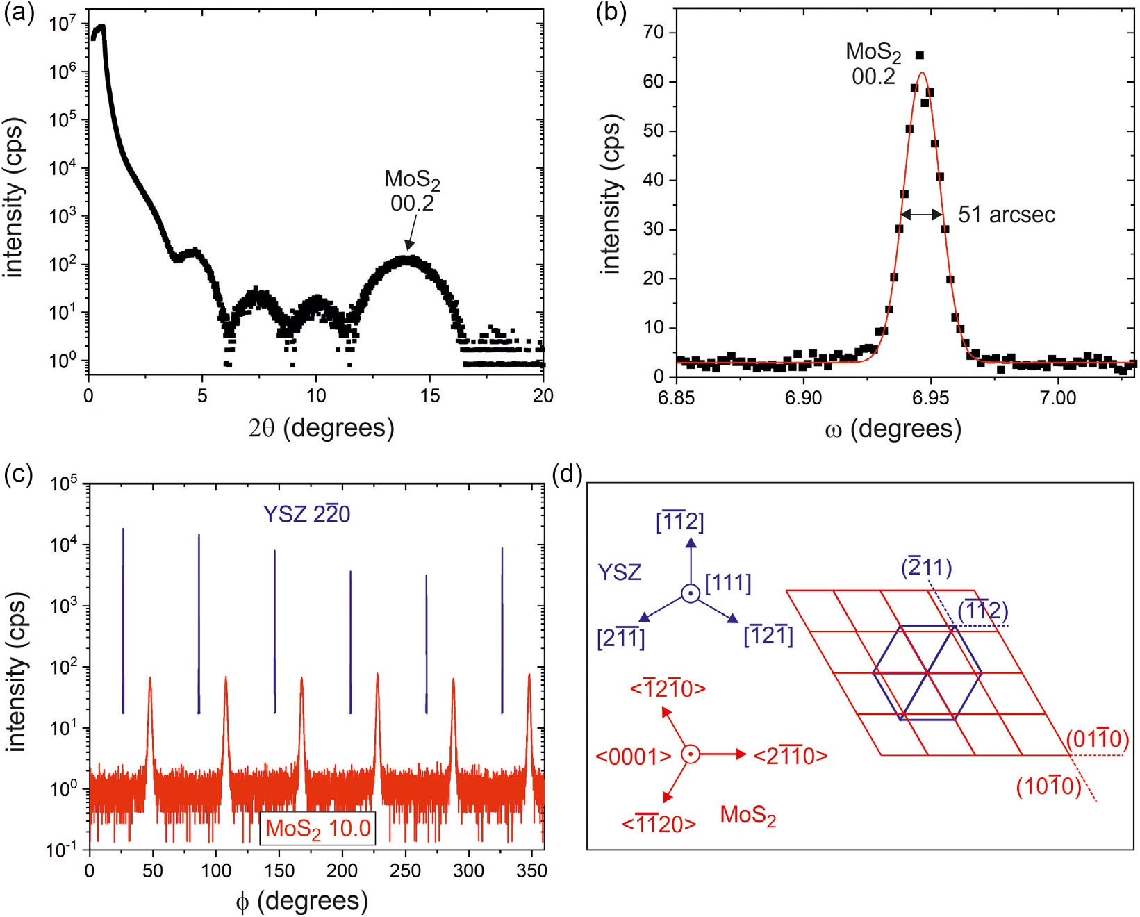
The multilayer samples were structurally characterized using high-resolution X-ray diffraction. The corresponding out-of-plane measurements (2θ–ω scan) show a prominent peak at about 2θ = 14.0°, which can be assigned to the MoS2 00.2 Bragg reflection (Figure 1a). The resulting vertical lattice parameter of cexp = 12.7 Å is in approximate agreement with the literature value of cMoS2 = 12.3 Å.In the immediate vicinity of the Bragg reflection, pronounced thickness fringes are observed, indicating a rather smooth interface between the substrate and the layer. From the angular spacing of the fringes, we can determine a MoS2 film thickness of t = 34.8(7) Å, which corresponds to about five MLs. A rocking curve (ω-scan) carried out at 2θ = 14.0° (Figure 1b) shows a full width at half maximum value of about Δω = 51 arcsec, which is close to the experimental resolution of the instrument.

Figure 1. Structural properties of a 3.5 nm MoS2 layer grown by PVD on YSZ (111) wafer. a) Out-of-plane X-ray diffraction 2θ–ω scan in the vicinity of the MoS2 00.2 Bragg reflection. b) Corresponding experimental X-ray rocking curve (ω scan) at the MoS2 00.2 Bragg reflection fit with a Gaussian line profile (red line). c) GIXD in-plane X-ray diffraction rocking curves (ϕ-scans) of the YSZ wafer (blue) and the MoS2 layer (red), taken at 2θ = 32.9° (MoS2 10.0 Bragg reflection) and at 2θ = 49.7° (YSZ 220 Bragg reflection). d) Epitaxial relationship scheme of YSZ wafer (marked in blue color) and MoS2 layer (marked in red color).
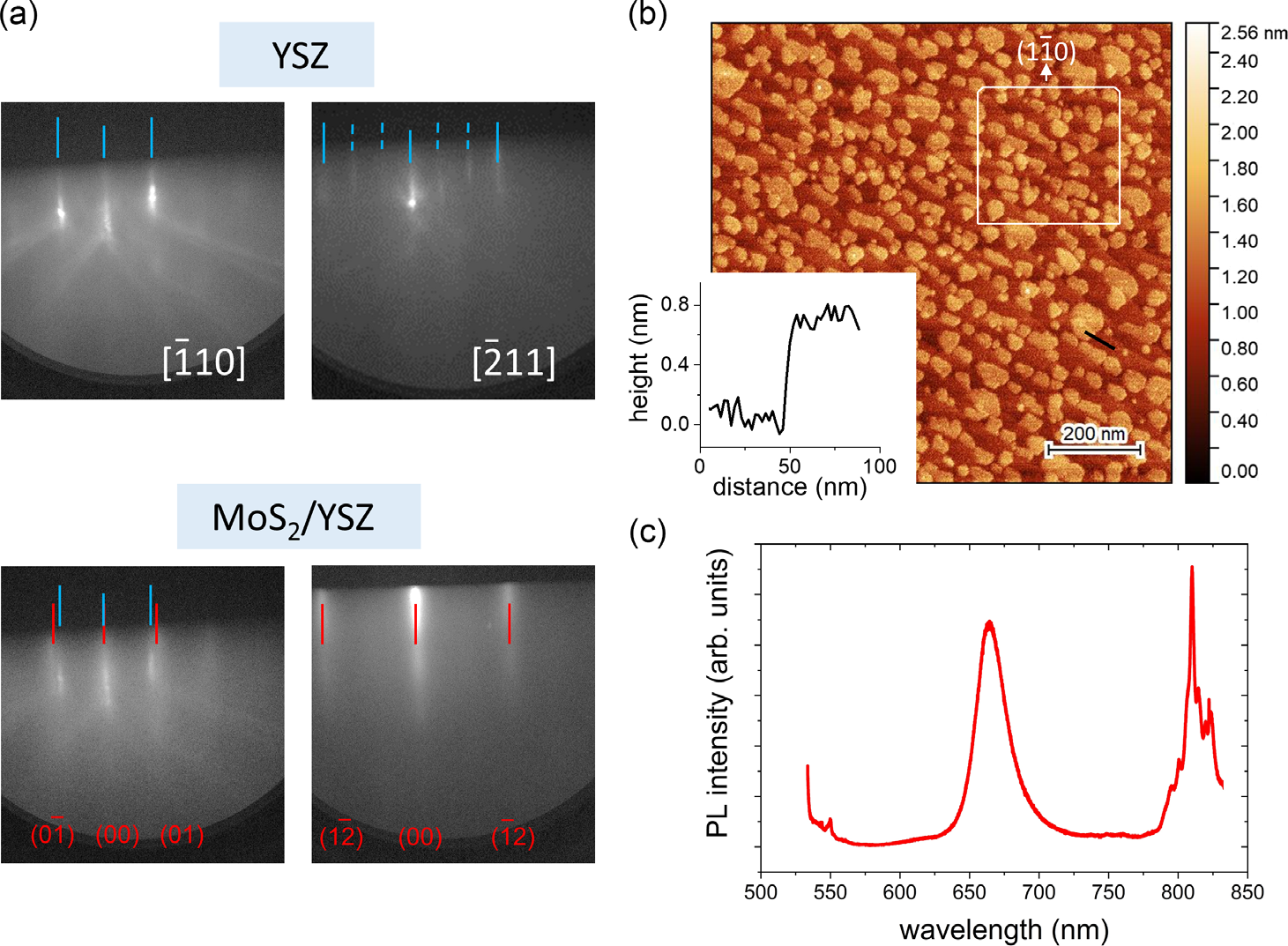
Decreasing the layer thickness down to 1 ML is expected to result in the appearance of a photoluminescence (PL) band, corresponding to the transition from the indirect to direct band in the 2H-polytype of MoS2.Figure 2a displays reflection highenergy electron diffraction (RHEED) patterns from the bare YSZ wafer (top) and after deposition of about 0.5 ML-thick MoS2 equivalent (bottom). The RHEED patterns show only one system of the streaky reflections from MoS2 (shown by the blue lines with corresponding Miller indices in Figure 2a), indicating a 2D growth mode and a clear epitaxial relationship with the substrate (reflections of the YSZ substrate are highlighted by the red arrows) with sixfold symmetry, as previously verified for the multilayer sample. The relative distance between the MoS2 streaks (blue lines) and the YSZ streaks (red lines) indicates that the MoS2 layer is relaxed already in the first monolayer.

Figure 2. Submonolayer thin MoS2 film grown by PVD on (111) YSZ. a) RHEED patterns of bare YSZ substrate (top, marked by blue lines) and MoS2 layer deposited on YSZ (bottom, red lines). The dashed lines correspond to the surface reconstruction. The RHEED patterns were recorded along the [110] and [211] directions of the YSZ wafer. The Miller indices of the MoS2 Bragg reflections (highlighted by red lines) are labeled. b) AFM image of the sample. The inset shows the in-plane orientation of the wafer and height profile along the black line. c) PL spectrum of the sample excited with a 532 nm laser line. The PL/Raman bands at 550 nm and 820 nm originate from the YSZ wafer.
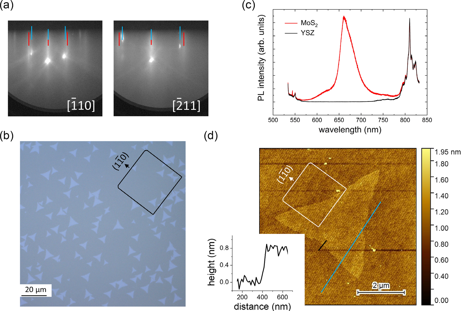
The chemical and thermal stability of YSZ in the form of a thin and flexible ceramic substrate planarized with SiO2 was recently demonstrated for CVD growth of few-layered MoS2 films using ammonium heptamolybdate and sodium hydroxide as precursors.In order to further prove the suitability of YSZ as a single-crystalline substrate for epitaxial growth of TMDCs, we performed a number of dedicated CVD growth experiments which are summarized in Figure 3. The layer orientation verified by RHEED coincides with that found in the PVD samples (Figure 3a). Optical microscopy reveals the formation of nonideal triangular MoS2 domains with a size of 5–10 μm (Figure 3b). The single ML thickness and the 2H-phase of the domains are con- firmed by PL measurements and AFM imaging. The PL spectrum of the sample shown in Figure 3c represents again a superposition of the signal from the layer and the substrate (red curve), while the measurements on the area in between the islands (black curve) depict the response of the substrate only. Optical microscopy clearly shows preferential in-plane epitaxial orientation of the islands. However, it is worth noting that antiparallel domains—that is, 180° domains—also show up. A closer inspection of the sample by AFM reveals that one of the zigzag edges of the MoS2 triangular is aligned perpendicular to the atomic steps of the wafer, appearing as a result of a substrate miscut of 0.2° toward the [110] direction (Figure 3d). Statistical analysis of optical microscopy images (Figure S4, Supporting information) reveals that this alignment holds for 93% of the domains.

Figure 3. MoS2 layer grown by CVD on YSZ (111) substrate. a) RHEED patterns of the sample recorded along the [110] and [211] directions of the YSZ wafer. Bragg reflections of the YSZ wafer and MoS2 are highlighted by the red and blue lines, correspondingly. b) Optical micrograph, demonstrating in-plane preferential orientation of 1 ML-thick MoS2 domains. c) PL spectra, from a MoS2 island (red curve) and from the bare substrate surface (black curve). d) Overview AFM image of the triangular domain and the height profile along the black line. The blue line depicts the direction of atomic step edges of the wafer.
3. Conclusion
We introduce Y-stabilized ZrO2 (111) as a commonly available wafer for the epitaxial growth of TMDCs. The material has been found to be applicable for both PVD and CVD growth processes. MoS2 layers grown on YSZ (111) with a small miscut toward the [132] and [110] directions exhibit sixfold symmetry and an inplane epitaxial relationship with the wafer of (1010) MoS2 || (211) YSZ according to GIXD and RHEED. Optical microscopy of the noncontinuous CVD layer reveals the presence of 180° rotation domains, as expected from epitaxial growth of a threefold material on a sixfold substrate. The observed similarity of the domain formation between sapphire and YSZ offers great opportunities for the fabrication of single-oriented TMDC layers on the substrate with smaller lattice mismatch by careful design of the wafer miscut orientation, combined with appropriate growth stoichiometry. The results are especially promising for the PVD process, where nucleation of MoS2 islands with a lateral size of up to 100 nm and strong PL as expected for 2H-phase of MoS2 in a single monolayer limit is observed already during the first growth runs.