In the present work, monocrystalline porous silicon was fabricated using the photoelectrochemical etching technique and then copper sulfide (CuS) nanoparticles were deposited on a porous silicon substrate at 250°C using spray pyrolysis method at different concentrations of CuS (0.1, 0.3 and 0.5M). The physical properties of CuS/PSi/c-Si heterojunction were studied. The results of photoluminescence (PL) exhibited that the peak position of PL spectra was shifted to the longer wavelength or lower energy when the concentration of CuS was increased. On the other side, the energy gap of CuS decreased with increasing concentration. The values of energy gap are 2.7, 2.59, and 2.55 eV at 0.1, 0.3 and 0.5M, respectively. The properties of the CuS/PSi/n-Si structure were enhanced.
1. Introduction
In recent years, many of papers have focused on nanostructured semiconductors, which have their unique structural properties. Copper sulfide (CuS) is a p-type semiconductor with direct energy gap of 1.6- 2.7eV. The composition of CuxS exists many stable phases. The composite Cu2S, the copper-rich, the diorlite, dignite, and anilite, ending with the covellite (CuS) phase, which is rich in sulfur. Copper sulfide thin films were deposited using many methods such as chemical bath deposition, sol-gel, chemical vapor deposition (CVD), chemical spray, and spin coating. The thermochemical spray pyrolysis method is considered the most common among the chemical methods for preparing thin films. These methods are summarized by spraying a solution of the material from which the film is to be prepared onto hot bases at a specific temperature that depends on the type of material used, as a thermochemical reaction occurs between the atoms of the material and the hot base, and as a result of this reaction a thin membrane is formed. Porous silicon (PSi) is a material with strong emissivity, showing effective illumination over a wide spectral range. Many research works have focused on porous silicon and is based on optoelectronic techniques such as light-emitting diodes, wave vectors, and photovoltaic diodes. The mixture between CuS thin film and PSi layer can provide an excellent homogenous of lattice constant.
2. Experimental Work
Figure (1a) exhibits a schematic diagram of the anodization etching method. In this work, there are two orientations; (100) and (111); of n-type silicon wafers are used with resistivity of 0.01-0.02 Ω.cm and the thickness of the silicon wafer is 505±12µm. The Si wafers were cleaned before the etching to remove any contamination on the surface.
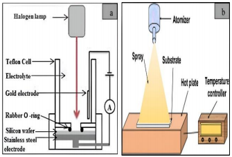
Fig. (1) (a) Diagram of adonization process, (b) diagram of chemical spray
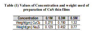
The hydrofluoric acid (16 wt.%) contraction has been diluted by using an absolute ethanoic solution (99%) (C2H5OH) to minimize the hydrogen bubbles during the etching. Fixed current density was maintained at 15 mA/cm2 and etching time of 5, 10 and 15 min were used. Additionally, a tungsten lamp of 100 mW/cm2 intensity was carried out. The set-up consists of two electrodes, the first part is gold and is connected to the acid solution (HF), the second part is a stainless-steel put under the Si substrate. After that, CuS/PSi heterojunction was achieved by using spray pyrolysis process. We used aqueous solution of copper chloride and sodium sulfide (Na2S) at various concentrations. We mixed first in distilled water (H2O) and then sprayed on the substrate in order to obtain ions of copper and sulfide. The CuS nanoparticles were deposited on PSi substrate at 250°C using spray pyrolysis method at different concentrations of CuS (0.1, 0.3 and 0.5M). The spray rate was used at 25 mL/min. The distance between the nozzle and the sample were fixed about 30 cm and a k-type thermocouple was used as shown Fig. (1b) and table (1).
3. Results and Discussion
The PL spectra shown in figures (2) and (3) are for CuS/Psi heterojunctions prepared at etching time of 15 min with fixed current density (15 mA/cm2 ), concentration of HF (18%) and concentration of CuS (0.1M and 0.5M) with orientation (100) and (111). Obviously, the strong emission peaks of CuS/PSi at orientation (100) were observed at 577.5 nm, 535.3 nm and 546.4 nm (green region) corresponding to energies of 2.19 eV, 2.31 eV and 2.27 eV of pure PSi and concentration 0.1 and 0.5M respectively (Fig. 2).
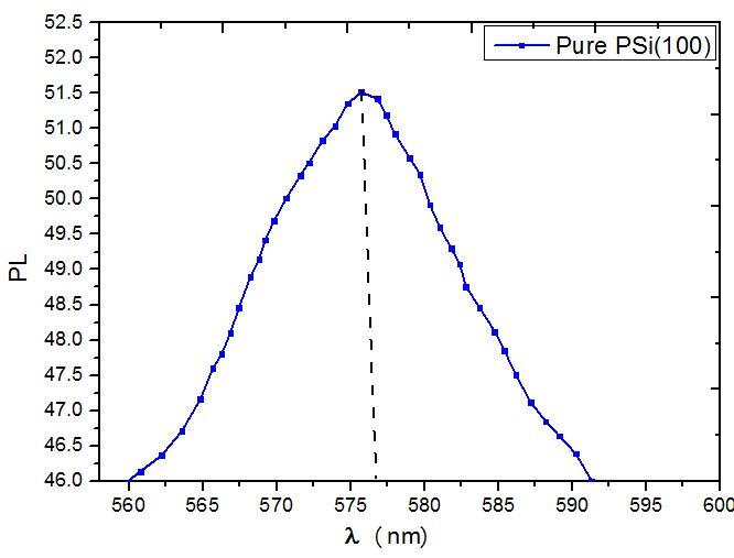
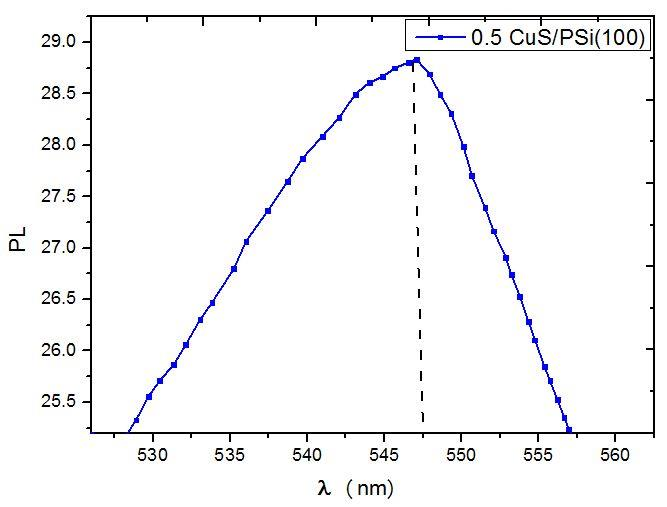

Fig. (2) PL spectra of CuS/PSi nanostructures fabricated at concentrations of (a) 0.1M, (b) 0.3M, (c) 0.5M of orientation (100)
In the same way, the PL emission peaks at orientation (111) were illustrated at 566.5 nm, 577.2 nm and 605.6 nm (green region) corresponding to energies of 2.15 eV, 2.14 eV and 2.04 eV of pure PSi and concentration 0.1 and 0.5M, respectively (Fig. 3) because of the carriers restricted (electron-hole) recombining in the PSi surface, and this is further supported by measurements of the particle sizes' statistical distribution. The peak position was shifted to the long wavelength or lower energy with increasing concentration of CuS due to the density of state of PL and the absorbance of the carriers due to quantum confinement effects. It can be seen the change in the peaks intensity due to the increasing of the number of smaller nanocrystallite sizes contributes to the PL since it generates more holes for further reactions as in tables (2) and (3). The silicon atoms near the crystallite's surface modify their bonds and dimension to adapt variations in the immediate environment, forming the recombination centers. The possibility of electron and hole recombination is a less dimension structure as the energy gap decreased with increasing concentration due to the confinement of PSi practical in a smaller dimension.
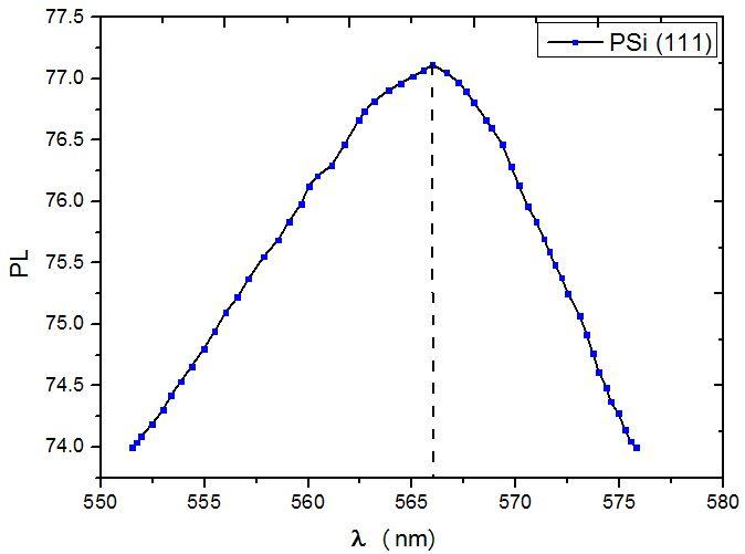
Fig. 3
4. Conclusion
In summary, CuS nanostructures were successfully deposited on porous Si wafer using chemical spray method. The peak position of photoluminescence was shifted to the long wavelength or lower energy when the concentration of CuS was increased. The energy gap increases with increasing concentration of CuS. Consequently, the experimental circumstances can be used to control the size and shape of the final structures. In brief, the characteristics of CuS/PSi photodetectors are effectively dependent on fabrication requirements.
上一篇: 石英晶体的蚀刻:综述
下一篇: 用于 MEMS 应用的玻璃湿法蚀刻:综述