Abstract
Tantalum films incorporated into superconducting circuits have exhibited low surface losses, resulting in long-lived qubit states. Remaining loss pathways originate in microscopic defects which manifest as two level systems (TLS) at low temperature. These defects limit performance, so careful attention to tantalum film structures is critical for optimal use in quantum devices. In this work, we investigate the growth of tantalum using magnetron sputtering on sapphire, Si, and photoresist substrates. In the case of sapphire, we present procedures for growth of fully-oriented films with α-Ta [1 1 1] // Al2O3 [001] and α-Ta [1 -1 0] // Al2O3 [1 0 0] orientational relationships, and having residual resistivity ratios (RRR) ~ 60 for 220 nm thick films. On Si, we find a complex grain texturing with Ta [110] normal to the substrate and RRR ~ 30. We further demonstrate airbridge fabrication using Nb to nucleate α-Ta on photoresist surfaces. Superconducting resonators patterned from films on sapphire show TLS-limited quality factors of 1.4 ± 0.3 x 10⁶ at 10 mK. Structural characterization using scanning electron microscopy, X-ray diƯ raction, low temperature transport, secondary ion mass spectrometry, and transmission electron microscopy reveal the dependence of residual impurities and screw dislocation density on processing conditions. The results provide practical insights for fabrication of high-performing technological devices including qubit arrays, and guide future work on crystallographically deterministic qubit fabrication.
Introduction
Studies of two level systems (TLS) in superconducting qubit devices have sought the microscopic origins of qubit decoherence.1-3 Although atomic displacements in junction oxides are the best understood TLS, recent work highlighting the role of surface oxides, hydrides and microfractures illustrates the complexity of the problem.4-6 Overall, most posited decoherence sources argue for the development of superconductor films with high quality oxides and uniform crystal structure.
Recent demonstrations of high-performance qubits fabricated largely using tantalum have drawn interest to materials science considerations particular to this superconductor.The apparent performance advantage over more conventional metals (such as Al and Nb) has been attributed to both the surface cleanliness enabled by tantalum’s resistance to corrosive cleaning agents (e.g., piranha solution) and also its favorable native oxides which exhibit low loss and magnetism.The growth of superconducting Ta films with controlled microstructure is therefore of paramount interest for the fabrication of qubits with minimal dissipation.
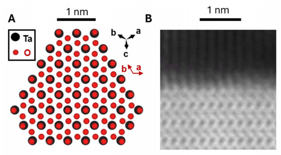
Growth of Ta on sapphire structurally follows the model of Nb.Sapphire permits epitaxial growth at the elevated temperatures at which the α-phase forms readily.Like Nb, coherent epitaxy of bcc Ta can occur on the a- and c-planes of sapphire.For 100 nm-scale film thicknesses as often used for circuits, the [110] Ta films that form on the sapphire a-plane show uniaxially elongated grain texture.On the c-plane, Ta also can grow in the [110] direction, but exhibits significant lattice mismatch, leading to the formation of columnar grains which are elongated along the sapphire [100], [010], or [110] directions. At higher temperatures or reduced background pressure, Ta grows in the [111] direction with a single azimuthal orientation, α-Ta [1 -1 0] // Al2O3 [100], equivalent to α-Ta (-1 1 0) // Al2O3 (2 -1 0).25 The lattice mismatch between the trigonal interfacial lattices is 1.9 % as illustrated in Fig. 1A.

Fig1
Table 1 summarizes results of Ta depositions on sapphire substrates using a range of magnetron sputtering deposition parameters. The sequence of depositions aimed to optimize parameters to minimize the film resistivity, which is a useful proxy for the density of scattering sites in the film, including the presence of impurity β-Ta secondary phase. Sample Sph 0 was grown by Star Cryoelectronics Inc., whereas the others were deposited at LLNL in the system described in Ref. . The clearest trend in this growth series is the eƯ ect of the chamber condition. The sample pairs Sph 4/5, Sph 6/7, Sph 8/9, and Sph 11/12 were each grown identically and immediately in sequence, and, in each case, the second deposit was appreciably more conductive (lower ). This indicates that with each successive deposition, the chamber environment becomes cleaner, leading to fewer scattering sites in the Ta. These observations are of considerable practical value, as they allow us to estimate the relative eƯ ects of growth conditions versus chamber condition on film product. Following the MBE literature on Ta epitaxy,20 we anticipated obtaining the highest quality films at the highest growth temperatures, but instead found increased resistivity at 800 °C, possibly due to chamber outgassing.Although the chamber history eƯ ect makes precise optimization challenging, low DC sputtering power, PDC < 150 W and a temperature of 625 °C were close to optimal for highly conductive films, approaching the bulk resistivity (13.5 μΩ-cm).
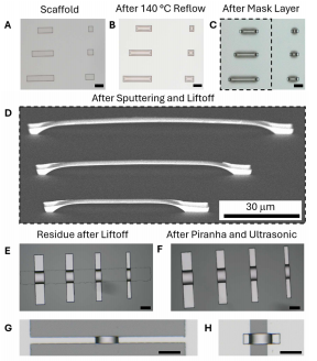
Fig. 2 shows the procedure for airbridge fabrication. First, a template structure on sapphire is formed using two AZ1518 photoresist layers. The first layer of resist is spun to a thickness of 2 μm, baked at 90 °C and patterned into rectangles defining the ‘scaƯ old’ of the bridge (Fig. 2A). The sample is then heated (‘reflowed’) at 140 °C for five minutes to round the scaƯ old (Fig. 2B). Next, another 2 μm layer of AZ1518 is spun and patterned to form the rectangular windows defining the perimeter of the bridge. The final template structure is shown in the optical image in Fig. 2C.

Fig2
We have demonstrated suitable growth conditions for high-quality Ta films with low densities of scattering defects on technologically important substrates, including Si, sapphire, and photoresist. The results bear upon many of the diverse microfabrication applications of Ta films, including qubit fabrication.40 For qubits, the demonstration of growth on polymer substrates allows for fabrication of piranha-compatible airbridges, enabling a convenient and high-performance workflow for multi-qubit fabrication.In these suspended airbridge structures, the nature of the film underside is of continued interest, and losses associated with this surface may be tied to eƯ ective removal of the nucleating species.
上一篇: 用于 MEMS 应用的玻璃湿法蚀刻:综述