ABSTRACT
Silicon dioxide (SiO2) is ubiquitous in biomedical diagnostics and other applications as a capture medium for nucleic acids and proteins. Diagnostic devices have seen rapid miniaturisation in recent years, due to the increased demand for portable point-of-care diagnostics. However, there are increasing challenges with incorporating SiO2 nanostructures into diagnostic devices, due to the complexity of nanostructured SiO2 synthesis, often involving etching and chemical vapour deposition under high vacuum conditions.
We report a novel and straightforward method for deposition of high-quality, nanoscale SiO2 films and 3D SiO2 structures using thermal decomposition of polydimethylsiloxane (PDMS), in a furnace at atmospheric pressure at 500℃. This method allows individual nanometre controllability of conformal pinhole-free layers on a variety of materials and morphologies. The temperature ramp rate is a key factor in determining the SiO2 deposit morphology, with slower ramp rates leading to highly conformal 2D films and faster ones yielding 3D nanodentrite structures. For the 2D films, the film thickness, as determined by spectroscopic ellipsometry and confirmed by SEM data, is shown to correlate excellently with initial PDMS source material mass in the thickness range 0.8–18 nm. Fits to ellipsometry models confirm that the refractive index of the deposited film matches the expected value for SiO2, while electrical breakdown measurements confirm that the breakdown strength of the films is comparable to that of high-quality thermal oxides. Depositions on high aspect ratio ZnO nanostructures are shown to be highly conformal, leading to core-shell ZnO-SiO2 nanostructures whose shell thickness is in excellent agreement with the expected values from deposition on planar substrates. At faster ramp rates an abrupt morphological transition is seen to a deposit which displays a 3D nanodentrite morphology. The possibilities for applications of both morphologies (and core-shell combinations with other nanostructured materials) in biosensing and related areas are briefly discussed, and the DNA capture capabilities of each nanostructure are measured. The high aspect ratio nanodendrite structures allow for significant DNA capture within microfluidic devices in the presence of low DNA concentrations, with a maximum average capture efficiency of 43.4 % achieved in the presence of 10 ng/mL of DNA, which is an improvement by a factor of ~ 3 over planar Si surfaces. Improvements by factors of >10 over planar surfaces were achieved at higher DNA concentrations of 100 and 1000 ng/mL.
Introduction
Silicon dioxide (SiO2) is one of the most widely utilised materials in biomedical and related applications, due to its relative biocompatibility and affinity for DNA and protein interactions compared to other commonly used materials like gold and silver. However, incorporating SiO2 materials and structures into portable, lab-on-a-chip (LoC) based technologies has proved challenging. Traditionally, lab based nucleic acid detection is performed using SiO2 microbeads, however, incorporating these microbeads into microfluidic channels produces inconsistent and irreproducible results. Recently, there has been a shift towards the use of Si and SiO2 micropillars in microfluidic LoC and biosensing devices to overcome these challenges . These micropillars are not only useful for DNA analysis, but a variety of other applications in areas like cell biology, targeted drug delivery , and photovoltaics etc.
It is clear that micro- or nanostructuring of the SiO2 will increase the surface area per unit volume of material and this is a particularly promising route for exploration in this area of materials science. However the creation of SiO2 nanostructured deposits is quite challenging, due to the complexity of SiO2 deposition and structuring methods, often involving etching and chemical vapour deposition (CVD) under high vacuum condition.
By contrast, other metal oxide materials, notably ZnO, readily form a variety of high surface to volume ratio nanostructured morphologies using both chemical bath and physical vapour deposition methods, in a self-assembled bottom-up manner. However, the surface properties of ZnO differ significantly from SiO2, and hence their interaction with biological species such as nucleic acids and proteins is quite different to that of SiO2.
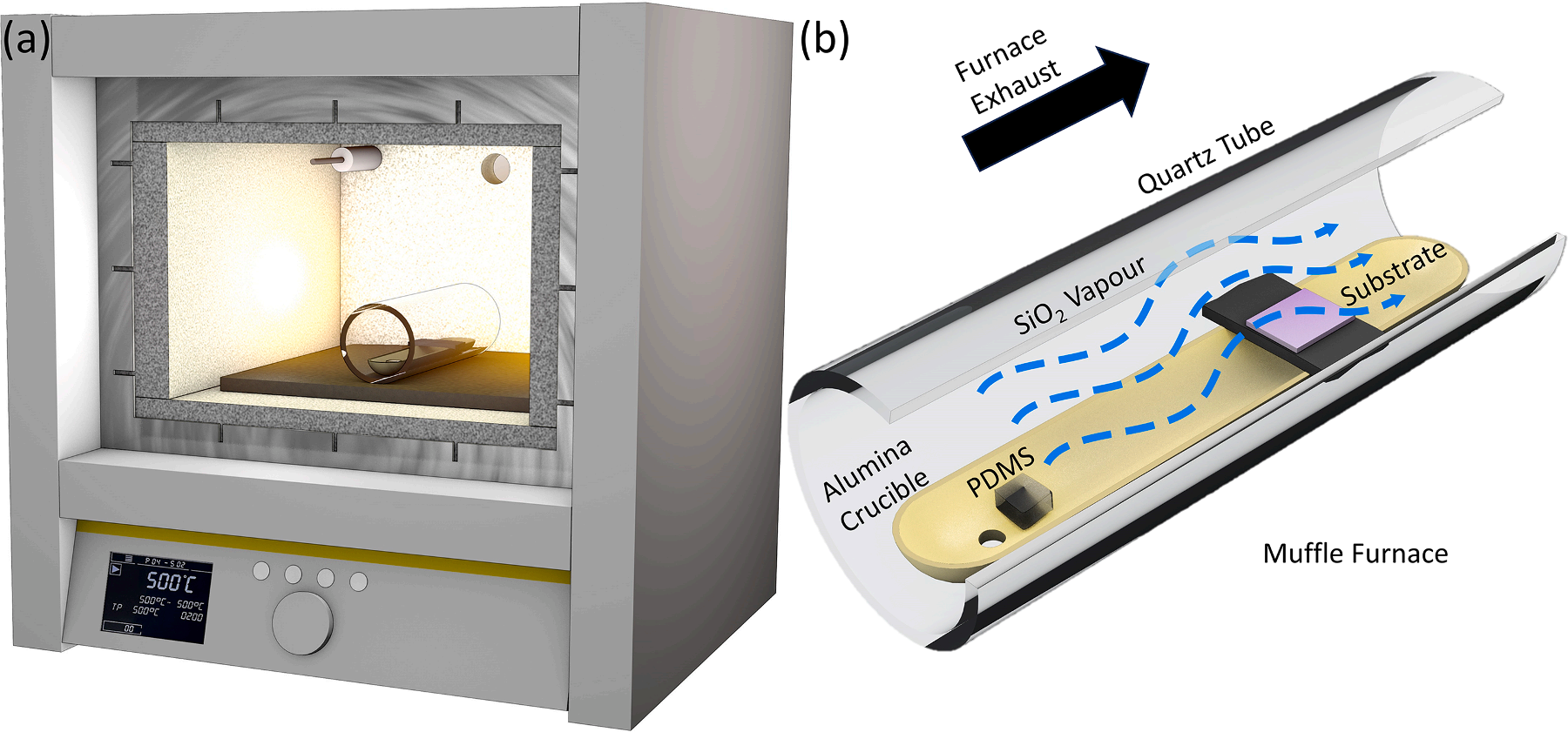
Planar substrates (both Si wafer coupons and ZnO thin films), as well as ZnO nanostructured deposits were coated in SiO2 using a novel PVD technique developed by our group, which is based on the thermal decomposition of polydimethlysiloxane (PDMS) in air. The technique is similar to that reported in our previous work, but with some slight differences which enable nanometre-scale control of film thickness, and also deposit morphology. To briefly summarise, varying masses of PDMS were placed at one end of an alumina crucible, with the substrates positioned at the opposite end, 5.5 cm away from the block of PDMS, lying across the boat in the manner shown in Fig. 1. This alumina boat was positioned inside a hollow quartz tube (3.8 cm inner diameter), and the quartz tube was placed in the centre of a muffle furnace (Nabertherm Muffle Furnace LT 3/11/B410), with the samples to be coated located between the PDMS block and the furnace exhaust. For the case of substrates ≤ 1 cm2 , which were too narrow to be suspended across the alumina crucible, we placed substrates on top of a larger Si wafer piece which was suspended across the crucible. The furnace was heated to 500 ◦C using ramp rates from 1 ℃/min up to 40 ℃/min, and this temperature was maintained for two hours. The amount of deposit is controlled by the PDMS mass. The temperature ramp rate allowed us to control the deposit morphology, with slower ramp rates leading to highly conformal 2D films with an abrupt transition at a heating rate of > 2℃/min to deposits with 3D nanodentritic morphologies.

Fig1
The experimental configuration is largely similar to that reported in our previous work . In that previous work small pieces of Si were used to mark portions of the substrate during growth to enable subsequent profilometry measurements of SiO2 deposit thickness. Using this method we determined using contact profilometry that 6 mg of PDMS, heated to 500℃ at a rate of 1 ℃/min provides an SiO2 thickness of 25-50 nm. Since that work we have altered our standard characterisation protocols to use spectroscopic ellipsometry (SE) to routinely measure deposit thicknesses, with occasional use of FESEM to confirm the SE measurements. The removal of the masking Si pieces has had a significant effect on the vapour flow close to the substrate and had led to a significantly reduced deposition rate, allowing much thinner films to be deposited with thicknesses as low as 0.8 nm, as shown below.
Results and Discussion
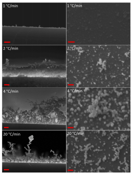
We have examined the effect of changes in the ramp rate of the furnace from 1 ℃/min up to 40 ℃/min in our new growth configuration, since previous work has established that the temperature ramp rate is a significant parameter in the decomposition of PDMS. Since the products of the thermal decomposition of PDMS depend on the temperature ramp rate, this affects the degree of depolymerisation. SEM data for these studies is shown in Fig. 2 below, in both plan view and cross-sectional view.
At a heating rate of ~ 2–3 ◦C/min however a sharp change in the deposit morphology is seen, whereby the deposited material no longer forms a thin planar film but rather a nanoscale 3D dendritic structure. We have explored heating rates up to 40 ℃/min and the dendritic morphology is observed up to the maximum heating rate obtainable in our furnace (40℃/min). Previous studies of the thermal degradation mechanisms of PDMS report that PDMS will form ceramic silicon oxycarbide at high heating rates. However, EDX analysis of the SiO2 structures shown in Fig. 2 and the ESI (Fig. S.2) confirms pure SiO2 stoichometry, with 20 and 40 ◦C/min dendritic structures having Si:O ratios of 1:2.1 and 1:1.9 respectively.

Fig. 2
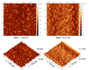
AFM data of these SiO2 thin films are shown in Fig. 4, as well as data from a thermal oxide provided by an industrial partner. The data for PDMS-based depositions are quite featureless, speaking to the flat, thin film morphology, which is confirmed by the cross-sectional FESEM data of the Au/SiO2 structure shown in Fig. 5 (the residual roughness in these images being due to the granularity of the Au layers).

Fig. 4
Conclusions
We have demonstrated a novel and straightforward method for deposition of high-quality, nanoscale SiO2 films and 3D SiO2 structures using thermal decomposition of polydimethylsiloxane (PDMS), in a furnace in atmospheric pressure at 500℃. The temperature ramp rate is a key factor in determining the SiO2 deposit morphology, with slower ramp rates leading to highly conformal 2D films and faster ones yielding 3D nanodentrite structures.
Detailed characterisation using SE, SEM, STEM, FESEM and XPS confirm that this method allows individual nanometre controllability of conformal pinhole-free layers on a variety of materials. For the 2D films the film thickness, as determined by spectroscopic ellipsometry and confirmed by SEM data, is shown to correlate excellently with initial PDMS source material mass in the thickness range 0.8–18 nm.