Abstract: This study examined the impact of temperature optimization on indium tin oxide (ITO) films in monolithic HJT/perovskite tandem solar cells. ITO films were deposited using magnetron sputtering at temperatures ranging from room temperature (25℃) to 250℃. The sputtering target was ITO, with a mass ratio of In2O3 to SnO2 of 90% to 10%. The effects of temperature on the ITO film were analyzed using X-ray diffraction (XRD), spectroscopic ellipsometry, and sheet resistance measurements. Results showed that all ITO films exhibited a polycrystalline morphology, with diffraction peaks corresponding to planes (211), (222), (400), (440), and (622), indicating a cubic bixbyite crystal structure. The light transmittance exceeded 80%, and the sheet resistance was 75.1 Ω/sq for ITO deposited at 200℃. The optical bandgap of deposited ITO films ranged between 3.90 eV and 3.93 eV. Structural and morphological characterization of the perovskite solar cell was performed using XRD and FE-SEM. Tandem solar cell performance was evaluated by analyzing current density-voltage characteristics under simulated sunlight. By optimizing the ITO deposition temperature, the tandem cell achieved a power conversion efficiency (PCE) of 16.74%, resulting in enhanced tandem cell efficiency.
1. Introduction
The global photovoltaic (PV) market is predominantly led by crystalline silicon (c-Si) solar cells, which constitute over 95% of the market share, however, in the dynamic of the PV sector, new photovoltaic materials are continually emerging, with perovskite standing out as a promising alternative to Si-based solar cells for its versatile applications in solar cells, LEDs, and even electrochemical water splitting, showcasing its growing importance in optoelectronics and beyond. Recent advancements in perovskite solar cells (PSCs), with an efficiency ranging from 3.13% to 26.1% between 2009 and 2023, underscore their potential as a cutting-edge solar technology. The Shockley–Queisser limit represents the maximum theoretical efficiency that a single-junction solar cell can achieve based on thermodynamic principles which is about 33.7% for a single-junction solar cell under standard test conditions; it is determined via the balance between photon absorption and thermalization losses. Integrating perovskites with crystalline silicon (c-Si) solar cells offers significant promise, surpassing the Shockley–Queisser limit for single-junction solar cells and boosting power conversion efficiency (PCE), thereby driving down the cost of electricity in photovoltaic systems. Jacak et al. also emphasized the inherent limitations of p-n junction solar cells, defined by the Shockley–Queisser limit. At the same time, they highlighted the innovative potential of perovskite solar cells to overcome these limitations. Third-generation cells, such as perovskite cells, achieve efficiencies comparable to p-n junction cells. Furthermore, they can enhance operational efficiency by up to 40% through the use of low-cost metallization, low-temperature processing, and simple manufacturing techniques, rendering them a competitive solution for future large-scale applications.
2. Materials and Methods
ITO films deposited at different temperatures (RT, 150 ℃, 175℃ , 200℃, 225℃, and 250℃) on soda-lime glass (surface: 2.5 × 2.5 cm2 , thickness: 1.1 mm) to investigate their structural, optical, and electrical properties. In the manufacturing process of the HJT solar cell, the temperature of the ITO layer is automatically regulated using temperature sensors and heaters. This automated control ensures precise and consistent temperature conditions, which are crucial for achieving the desired material properties and device performance. The films were deposited using direct current (DC) magnetron sputtering integrated into a physical vapor deposition (PVD) system (Meyer Burger Technology AG, Thun, Switzerland) operating at 13.56 MHz. A 99.999% (5N) purity ITO sputtering target (Kurt J. Lesker Company, Jefferson Hills, PA, USA) was employed for the film deposition process, resulting in ITO films with a thickness of 100nm.
Prior to placing the glass substrates into the PVD chamber, they were cleaned in ultrasonic baths containing acetone for 5 min, ethanol for 5 min, and distilled water for 10 min, followed by drying with nitrogen (N2) gas. The cleaned substrates were then introduced into the PVD system, and the system was allowed to reach a working pressure of 7.3 × 10⁻⁶ mbar. A deposition pressure of 2.1 × 10⁻² mbar was maintained by continuously supplying argon (Ar) and oxygen (O2) to the chamber. Oxygen O2 gas was introduced during the sputtering process to control the stoichiometry of the deposited ITO film. The presence of oxygen accelerated the oxidation process and created the desired crystal structure. By adjusting the ratio of oxygen to argon gases, the oxygen content in the ITO film can be finely tuned, which is critical for achieving the desired electrical and optical properties. ITO films were deposited via DC magnetron sputtering at different temperatures while keeping the gas ratios (Ar: 200 sccm and O2: 3.3 sccm) and power (1850 W) constant. To prevent contamination, the system was initially operated in a vacuum before loading the substrates, and the process was then carried out. Table 1 shows these deposition parameters and their corresponding notation.
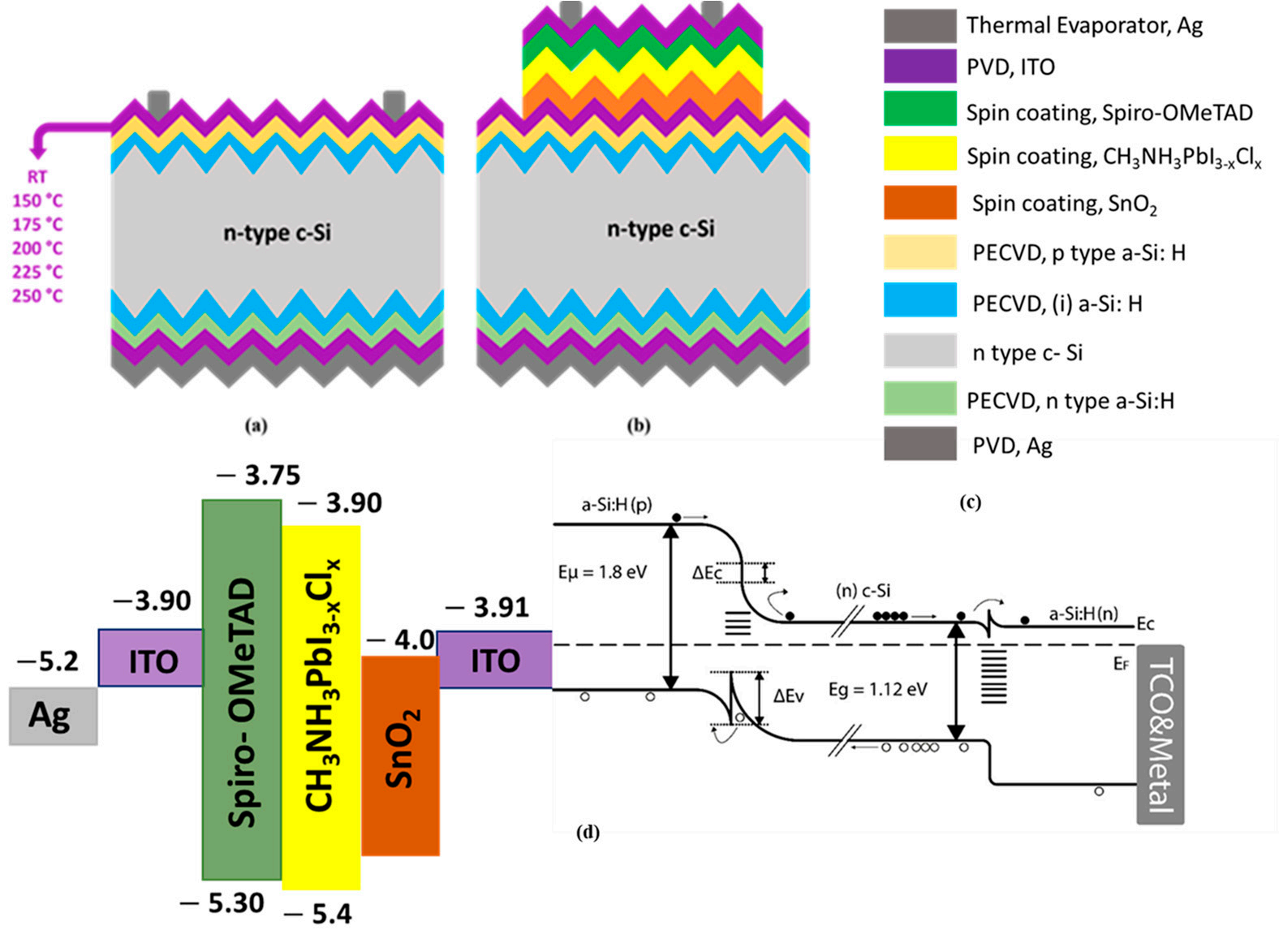
On the rear surface, deposition of the n-type a-Si: H layer was followed by the deposition of 40 nm ITO and 220 nm silver (Ag) layers using the PVD system. After coating the p-type a-Si: H layer, the front surface coatings were completed with the deposition of ITO films at different temperatures. Finally, finger and busbar patterns were printed on the front surface of the HJT solar cells using Ag paste via the screen print method (ASM Assembly Systems, Munich, Germany), and the solar cell was completed by firing it at 200℃ for 10 min. Figure 1a provides a schematic representation and eV diagram of the HJT solar cell.

Fig1
The SnO, colloid solution was dissolved in 10uL of isopropanol with magnetic stirringfor 2h at room temperature. Subsequently, filtration was performed to remove particulatematter and impurities from the solution using a 0.45 um (PTFE) filter. The solution preparedon the spin coating was taken with the help of a pipette and then coating was performed onITO by rotating it at 3000 rpm for 30 s. After that, the coating was annealed at 150℃ for30 min. T'he material was then transferred to the glove box to apply a pervskite layer coatingBefore coating the perovskite on the coated ET'L, layer, it was heated at a low temperature onthe hot plate for a while. The ET'L layer was coated with a formulation ofCHNHPbs-Clin a molar ratio of 1:1:4 containing methylammonium iodide (MAl), PbCl and Pbl, in DMFThe coated layer was then heated on a hot plate at a low temperature of 60 °C for one hour.Next, perovskite solution was dripped onto the ETL layer through a 0.45 um (PTFE) filterand spun at 4000 rpm for 45s. Then, a 70°C annealing process was performed on a hot plateOnce the perovskite layer was annealed, it was allowed to cool down before the application olthe prepared Spiro-OMeTAD solution. Using the dyamic coating method, the solution wascoated at a speed of 4000 rpm for 30 s. Upon the completion of the monolithic tandem cell, noencapsulation procedure was implemented.
3. Results
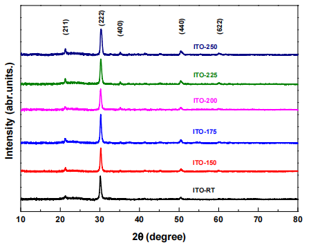
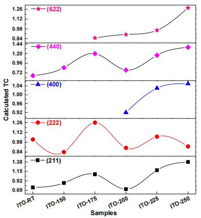
Figure 2 shows the XRD analysis of ITO films deposited at different temperatures (RT, 150, 175, 200, 225, 250 ◦C). ITO films were scanned by selecting the 2θ scanning range of 10 to 80◦ . According to the analysis, the diffraction peaks (211), (222), (400), (440), and (622) corresponded to cubic ITO. According to the analysis, the diffraction peaks (211), (222), (400), (440), and (622) corresponded to cubic ITO and all films showed polycrystalline properties. While the (400) peak was not visible in the ITO-RT, ITO-150, and ITO-175 samples, it was clearly seen when the temperature was applied above 175℃(Figure 2). This meant that the applied temperature treatment improved the arrangement of atoms, which lead to a better crystal structure. Table 2 shows the structural parameters of ITO films deposited at different temperatures. The structural parameters of ITO films were calculated according to the diffraction peak (222) plane of the highest intensity. It should be noted that the orientation of ITO (222) and (400) diffraction peaks can be changed by increasing the film ratio and temperature. According to (222) plane, the ITO-150 sample had the lowest full width half max (FWHM) value (7.18 × 10⁻³ rad), while the FWHM value of the ITO-250 was the highest (8.67 × 10⁻³ rad). In addition, a continuous increase was observed in the FWHM values of ITO films deposited above 150 ◦C as the temperature increased. The 2θ values of the all ITO-RT, ITO-150, ITO-175, ITO-200, and ITO-250 samples in the (222) orientation were found to be 30.14◦ , 30.23◦ , 30.22◦ , 30.19◦ , 30.25◦ , and 30.32◦ , respectively ((ICSD Card No: 98-005-0848 (ITO-RT, ITO-150, and ITO- 200), ICSD Card No: 98-005-0847 (ITO-175), and ICSD Card No: 98-005-0849 (ITO-225, and ITO-250)).

Fig2
The crystal size was calculated using Equation (1) where k is the shape factor (0.9)A is the X-ray wavelength, β is the broadening of the diffraction line peak at an angle of 20 at FWHM in radians measured using Gaussian distribution, and f is the Bragg angleTable 2 shows the crystal size and β values of ITO films deposited at different temperatures.It was observed that the crystal size and β values were inversely proportional, and theβ decreased clearly while the crystal size increased (Figure 3). In addition, as shown inTable 2, while a decrease in crystal size was observed with increasing temperature from150 to 250 'C, the best crystal size was determined as 20 nm at 150 °C. Although thisshows that ITO samples crystallize better at 150 °C, different characterization methods areneeded since the values were very close to each other.

Fig3
In conclusion, this study investigated the effects of temperature optimization on theITO film in the subcell of a monolithic HT/perovskite tandem solar cell architecture.Through optimization, the optimal temperature for the ITO film within the subcell wasdetermined to be 200 °C, The efficiency of the Tandem-200 configuration was found to be16.74%, which represented a significant improvement over the eficiency of the Tandem-Rlcon figuration, which stood at 15.78%. The optimization of the temperature in the subcellresulted in an increase in efficiency of approximately 1%. The light transmittance exceeded80% and the sheet resistance was 75.1Ω/sq for ITO deposited at 200 °C. Analysis revealedthe presence of structural defects and pinholes in the perovskite top cell, as well as areason the textured surface of the HT bottom cell where the perovskite did not uniformlycover. Additionally, while thicker layers of the perovskite top cell initially enhancedlight absorption, they also introduced various limiting factors, including increased self.absorption, losses in charge transport, optical losses, and stability issues. The presence ofpinholes, defects, and thick cell structures collectively impaired the efficiency of monolithictandem solar cells. In general, the response of ITO to temperature changes has a directimpact on the overall performance and durability of tandem solar cells. Optimizing theelectrical and optical pmperties of ITO, as well as its thermal management capabilityenabled cells to operate at high efficiency. Minimizing temperature stress and expansionmismatches maintained the structural integrity of the cells and ensured their long lifetime.
Therefore, optimizing ITO against temperature effects is critical to improving the overall performance of tandem solar cells. Recent progress in silicon HJT/perovskite tandem solar cells has centered on optimizing the layers in both the top and bottom cells and incorporating innovative materials and diversifying the types of silicon cells used as the bottom layer. Future research can aim to develop commercially viable methods to improve the interface between HJT and perovskite solar cells, such as improving the TCO structures used as buffer layers and developing techniques to enable the homogeneous deposition of perovskite solar cells onto HJT solar cells.
下一篇: 通过芯片到晶圆混合键合实现多层芯片堆叠