Abstract—A collective die-to-wafer bonding flow is extended beyond the N=2 tier to the N=3 and N=4 tier by collectively bonding multiple layers of dies on top of a target wafer. The N=2 die-level is shown to be consistently free of bonding voids (bond yields close to 100%) with +99% die transfer yields. For the N=3 and N=4 die-levels, both the transfer yields and bonding yields are significantly lower. Both N=2 and N=3 stacks show similar die-totarget wafer alignment. A cross sectional SEM of a 5-micron pitch shows excellent alignment and connectivity between Die 1 and Die 2 (N=3).
I. INTRODUCTION
Certain 3D IC technologies require a vertical interconnect with high connectivity densities between dies. A high alignment accuracy follows and as such the choice of process favors a hybrid bonding process. Both collective die-to-wafer bonding and direct die-to-wafer bonding schemes are attractive in this regard. Where a direct bonding flow seems much less complex compared to a collective bonding flow, there remain limitations regarding die-level cleanliness. Much progress has been made though, by enabling a wafer level cleaning approach before die pick up. However, during the final pick-up step the sensitive bond surface will be in contact with the die-placement tool leading to very stringent tool-cleanliness requirements or in situ die-level cleaning capability. In contrast, a collective die-to-wafer bonding flow, although more complex, allows all processing on wafer-level tools and as such allows inspection of the die level bonding surface prior to bonding. In several previous reports, imec’s proposed flows were explained in detail. It was shown that very thin dies (50 µm) or thick dies (775 µm) can be transferred from a temporary carrier to a target wafer with transfer yields and bond yields close to imec. The choice of temporary carrier system will depend strongly on the die type. For ultra-thin and flat dies (50 µm) a silicon carrier system can be used that allows mechanical debonding of the dies with transfer yields up to unity.Mechanical debonding has the advantage of using silicon carriers. On the other hand, using glass offers the benefit of UVlaser debonding.
Whenever dies become either too thick, too warped or simply have a different backside, the final touch to the adhesive of the carrier system might be impacted. Finetuning adhesion to enable wafer level cleaning (without losing dies) and still allowing a mechanical peel debond often results in either a limited die transfer or extensive die damage.Solving dietemporary carrier adhesion issues can be time consuming and very die-dependent. As such a glass carrier was introduced for the final debonding step together with a laser release layer (LRL) on the dies. Although 100% die transfer could easily be achieved, 1-4% of the dies showed some damage during the process. A study was performed to assess potential laser damage to ultrathin dies. The main finding was that during the ablation process a shockwave is generated in the LRL that propagates to the thin die and leads to some damage at the corners of the dies. This damage can easily be avoided by separating the ablation interface from the die interface by either using a thick LRL or an additional temporary bond material (TBM) between the LRL and the die, (which we will call acoustic layer (AL). Using the latter methodology, 100% die transfer could be achieved with electrically yielding daisy chains and kelvin structures up to 80% for the 7-µm pitch range.
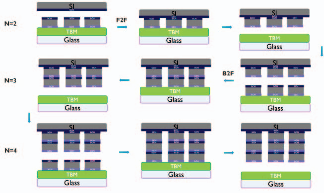
The robustness of this flow was demonstrated several times for the N=2 level, with N equal to the number of interfaces. Provided that the right dielectrics are present on the die backside, after die transfer the dies can be collectively cleaned and a second layer of dies can be bonded on top (Fig. 1). This step can be repeated X times to allow multi die stacking. In this publication the process of reference (POR) flow, using laser debonding and acoustic layer, is utilized to enable N=3 and N=4 stacks. As such a first layer of dies is transferred to the target wafer (tier 1) to enable N=2. During Tier 2 a second layer of dies is transferred on top of the first layer of dies to enable N=3 and finally Tier 3 to enable N=4. Both non-aligned bonding and aligned bonds are shown. Finally, an N=3 stack is prepared using electrically yielding dies in order to evaluate the connectivity between die 1 and die 2 using a cross sectional SEM of a 5-micron pitch connection.

Figure 1. Simplified flow for N=2, N=3 and N=4 collective die-to-wafer transfer.
The collective die-to-wafer flow consists of several parts: i) die preparation, ii) die pick and place, iii) bonding and iv) debonding. For the die preparation step, the wafer is flipped and mounted/bonded upside down to a temporary carrier using a temporary bonding system. The wafer is thinned down to 50 µm, and the backside surface is prepared. For the short loop experiments the temporary bond system was BrewerBOND 305 paired with BrewerBOND 510 material which allows for an easy mechanical release during the subsequent wafer flip step. A low temperature SiCN is deposited as backside bonding dielectric. For the full loop dies, presented in section IV, Brewer’s Versa layer system consisting of BrewerBOND C1301 and BrewerBOND T1107 was used. This system enables elevated temperature processing and much better CMP control during the preparation of the hybrid bond pads after TSV reveal. The details of the full loop die processing and results will be published elsewhere. After backside preparation the thin wafer is flipped again, this time to a glass carrier, and the frontside is thoroughly cleaned after which a photoresist is coated to protect the frontside dielectric. This wafer flip step and resist coating step has several functions: the resist protects the die-frontside from the tape used during dicing as well as from the dicing itself. The temporary bonding adhesive and laser release layer allow for a final flip onto tape frame to enable dicing. Both of the materials will be diced and re-used during the final collective die transfer step.
Four N=2 stacks were prepared and evaluated by calculating the transfer yields and bond yields. All prepared wafers had a transfer yield between 98-100% (Fig 3). The transfer yield is defined as the number of dies that were successfully transferred to the target wafer over the number of dies that were successfully populated on the temporary carrier. The bond yield (described in detail in [8]) is a measure of how void free the transferred dies are and are all close to 99%.

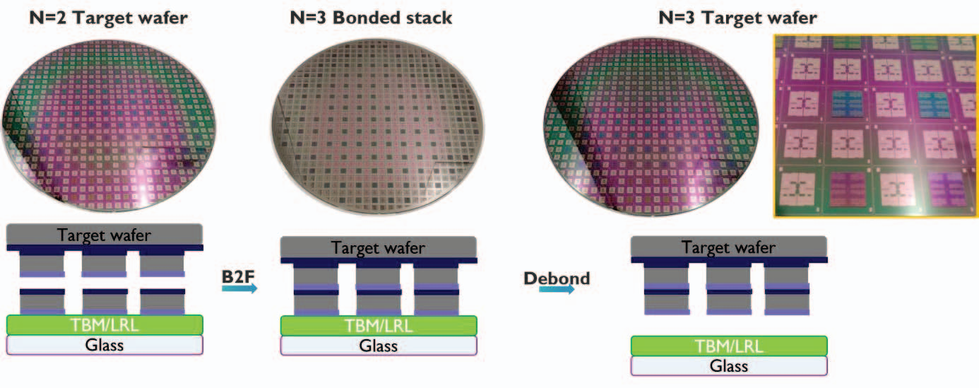
Figure 3. Simplified collective die-to-wafer bonding flow with pictures of the N=2 target wafer (after tier 1), the N=3 bonded stack and the N=3 target wafer (after tier 2).
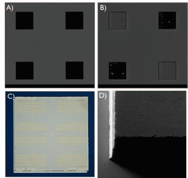
In the following step the four N=2 stacks were used to generate four N=3 stacks (Fig 3 & 4). In contrast to the Tier 1 transfers the transfer yields of Tier 2 vary strongly from stack to stack with the best result being 93% and the worst 64% (92% and 84% for the two others). The lower transfer yields are also reflected in lower bond yields (Fig 4 & 6). The bond yields range between 60% and 85% however, this data is misleading due to the non-transferred dies. Normalizing the bond yield over the number of transferred dies gives a more realistic number of the number of voids per transferred dies. These normalized bond yields range from 85 to 90%. This means that around 10-15% of the die area shows voiding indicative of a die-backside problem, caused either during back side processing or, more likely, an insufficient cleaning of the die backside after the Tier 1 transfer step. It is interesting to note that the bond yield of the Tier 1 layers (N=2) does not suffer from the Tier 2 step (Fig 4). Indeed, extremely limited voiding can be seen for the Tier 1 interface compared to the tier 2 interface (Fig 5 A&B). Due to the die thickness, after transfer of the second die-layer it is difficult to distinguish between a single die layer or a double die layer. The SAM measurement clearly reveals the missing dies (Fig 5B & 7). Further visualization of the double die stacks can be provided with IR microscopy (Fig 5C) and SEM imaging (Fig 5D).

Figure 5. A) SAM of N=2 interface, B) SAM of the N=3 interface, C) optical image of 2 misaligned dies, D) SEM of 2 well aligned dies.
V. CONCLUSIONS
Although a lot of work has been published in collective dieto-wafer bonding, truly little has been done on using this flow for multi-tier die stacking. Within this publication it is shown that the proposed imec collective-die-to-wafer bonding flow, including laser debonding with laser release layer and acoustic layer, can be extended to the multi-tier level. Although much optimization still needs to be done, mostly regarding die cleaning, several N=3 stacks were prepared with transfer yields up to 93% and bond yields up to 90%. Similar die-to-target wafer alignment results can be obtained as for the tier 1 level (Majority of the dies below 2 µm). Further extension to the N=4 level was less successful as the transfer yield decreased to 48% with much lower bond yield (~80%). Finally, an N=3 stack was built with hybrid bond pads and TSVs to evaluate the hybrid bond interface between die 1 and die 2 using cross sectional SEM, which shows excellent connectivity between the 2 dies for the 5 µm pitch.
下一篇: 湿度和表面粗糙度对晶圆直接键合的影响