ABSTRACT
Efficiently passivating germanium (Ge) surfaces is crucial to reduce the unwanted recombination current in high-performance devices. Chemical surface cleaning is critical to remove surface contaminants and Ge oxides, ensuring effective surface passivation after dielectric deposition. However, Ge oxides can rapidly regrow upon air exposure. To understand the surface evolution after wet cleaning, we present a comprehensive study comparing HF and HCl deoxidation steps on p-type Ge surfaces and monitor the surface as a function of air exposure time. Distinct oxide regrowth dynamics are observed: HF-treated samples exhibit swift regrowth of all Ge oxide states, whereas HCl-treated Ge surfaces exhibit a lower concentration of low degrees of oxidation and slower or no regrowth of high oxide states even after 110 min of air exposure. In addition, the presence of Ge–Cl bonds induces different oxidation dynamics compared to the Ge–OH bonds resulting from HF cleaning. This leads to varying surface electronic band structures, with HF-treated Ge exhibiting a strong positive band bending (þ0:20 eV). Conversely, HCl-treated samples display a lower band curvature (þ0:07 eV), mostly due to the presence of Ge–Cl bonds on the Ge surface. During air exposure, the increased GeOx coverage significantly reduces the band bending after HF, while a constant band bending is observed after HCl. Finally, these factors induce a reduction in the surface recombination velocity after wet etching. Combining both chemical and field-induced passivation, HF-treated Ge without rinsing exceeds 800 μs.
I. INTRODUCTION
Germanium (Ge) is used for many applications such as metal–oxide–semiconductor field-effect transistors (MOSFETs),free-standing membranes, IR lenses,biosensors,batteries,or multijunction solar cells.In most cases, high-performance device fabrication requires a proper understanding and control of the Ge surface passivation. Indeed, the potential of Ge is hampered by its high surface defect density. These defects lead to a high charge carrier recombination rate at the surface and can compromise the channel’s carrier mobility in MOSFET devices.In optoelectronic devices, such as solar cells and lasers, the electronic states induced by surface defects can act as nonradiative recombination centers for minority charge carriers and, therefore, decrease the device conversion efficiency.To counteract this detrimental surface impact on the final device’s performances, various passivation paths have been developed based on dielectric layer deposition.Although many of these studies were more interested in determining and optimizing the deposition parameters and the dielectric layers to obtain high passivation quality, some authors have mentioned the importance of the cleaning step performed prior to the deposition of the dielectric layer on the passivation performances.Ge wafers are traditionally exposed to wet cleaning to etch the native Ge oxide and prevent oxide regrowth. However, unlike on silicon, the peroxide-based solution cannot be used with Ge due to their high etching rates.From this observation, several cleaning techniques have been developed using water,ammonium hydroxide (NH4OH),thiols (–SH),or organic compounds.The cleaning step based on halogenated acid etchants (mostly, HF and HCl) has rapidly become widespread in the Ge industry by analogy with Si industrial cleaning steps.
In this work, we present a comprehensive comparison between HF and HCl cleaning procedures on p-type Ge (100) surfaces and elucidate the modification of both the surface composition and the electronic band structure after these treatments by parallel angle-resolved x-ray photoelectron spectroscopy (AR-XPS) measurements. In addition, their evolutions with air exposure dependence are clarified. Finally, we use microwave-detected photoconductivity (MDP) measurements to study the influence of these halide treatments and their relative surface modifications on the minority carrier lifetime.
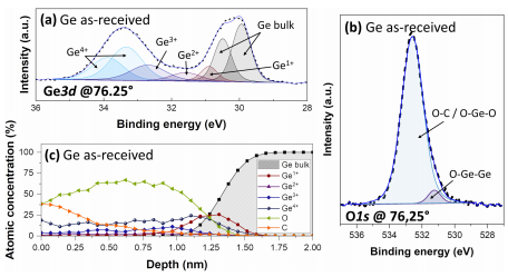
Preliminary AR-XPS experiments are performed on an as-received Ge substrate with its native oxide, hereafter referred to as Ge as-received. Figure 1(a) shows a typical XPS Ge3d core-level spectrum recorded at a collection angle of 76:25。. This spectrum has been decomposed into five contributions corresponding to Ge–Ge bonds from the bulk Ge and GeOx bonds corresponding to the four Ge surface oxidation states: Ge1þ, Ge2þ, Ge3þ, and Ge4þ. The Ge3d peaks related to Ge–Ge and Ge4þ bonds are fitted with a doublet using a spin–orbit splitting of 0.6 eV and an area ratio between the d5=2 and d3=2 components of 0.66. Due to the energy splitting of the Ge3d orbital, the doublet of the GeOx (1≤x≤3) peaks is not resolved, and these contributions are fitted with a single peak. The Ge3d5=2 peak associated with the bulk Ge–Ge bonds is located at 29.8 eV, while the peaks related to the Ge1þ, Ge2þ, Ge3þ, and Ge4þ oxidation states are shifted with respect to Ge3d5=2 to a higher binding energy by 0.8, 1.8, 2.6, and 3.4 eV, respectively.33 In addition to Ge, oxygen and carbon are detected on the Ge surface. The O1s peak [Fig. 1(b)] is fitted with two contributions located at 531.1 and 532.3 eV, which can be assigned to O–Ge–Ge and a combination of O–C and O–Ge–O (second neighbor effect) chemical environments,45 respectively, present in the native oxide and carbonaceous pollution. The reconstructed surface composition, calculated from the atomic concentration profile collected at various angles, is represented in Fig. 1(c). In addition to carbon contamination, the atomic concentration profile shows that the native oxide formed on the Ge surface is 1.5 nm thick (depth at which the atomic percentage of Ge Bulk is higher than 90%). The native oxide is mainly composed of Ge4þ except at the interface between the Ge oxide and Ge bulk, where the Ge1þ oxidation state dominates.

Fig1
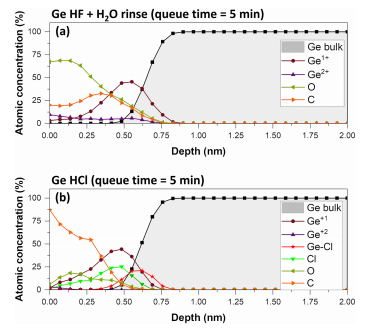
The reconstructed atomic concentration profiles after wet treatment [Figs. 4(a) and 4(b)] indicate that the surface layer is reduced to a 0.75 nm thickness and is mainly composed of Ge1þ for both treatments. In the case of HCl treatment, a Ge–Cl layer coexists with Ge1þ. These results confirm the capability of HF and HCl wet cleaning to remove the Ge native oxide. The evolution of the surface composition as a function of the air exposure time has been investigated by XPS. For both HF-treated and HCl-treated samples, the Ge3þ- and Ge4þ-related peaks are visible after 110 min of queue time (air exposure), associated with a noticeable increase in the thickness of the oxide layer up to about 1 nm [Figs. 5(a) and 5(b)]. In addition, the Ge–Cl bonds have been replaced by Ge–O bonds during the oxidation (confirmed by the disappearance of the Cl2p peak as showed in Fig. 8).

Fig4
The results presented in this study demonstrate that the cleaning procedure plays a critical role in the chemical composition, the surface band structure, the oxidation resistance, and the minority carrier lifetime of Ge. Our findings revealed varying oxide regrowth behaviors. For instance, Ge samples treated with HF exhibited a rapid regrowth of all degrees of oxidation, while those treated with HCl showed a reduced concentration of low degrees of oxidation following the cleaning and slower or negligible regrowth of high degrees of oxidation, even after 110 min of air exposure. This difference can be attributed to the presence of Ge–Cl bonds, which induce a distinct oxidation process compared to the Ge–OH bonds resulting from HF cleaning. As a consequence of these distinct surface compositions, Ge subjected to HF treatment with a water rinse displayed a pronounced positive band bending of þ0:20 eV. In contrast, HCl-treated samples exhibited a lower band curvature of þ0:07 eV, primarily due to the presence of Ge–Cl bonds on the Ge surface. Over the course of air exposure, an increase in the coverage of GeOx-based compounds led to a significant reduction in band bending after HF treatment, while HCl treatment maintained a consistent band bending. In summary, these factors collectively contributed to a reduction in the SRV after wet etching. By combining chemical and field-induced passivation, we achieved a minority carrier lifetime exceeding 800 μs in HF-treated germanium without rinsing.
上一篇: 湿度和表面粗糙度对晶圆直接键合的影响