ABSTRACT: Heat accumulation and self-heating have become key issues in microelectronics owing to the ever-decreasing size of components and the move toward three-dimensional structures. A significant challenge for solving these issues is thermally isolating materials, such as silicon dioxide (SiO2), which are commonly used in microelectronics. The silicon-on-insulator (SOI) structure is a great demonstrator of the limitations of SiO2 as the low thermal conductivity insulator prevents heat dissipation through the bottom of a device built on a SOI wafer. Replacing SiO2 with a more thermally conductive material could yield immediate results for improved heat dissipation of SOI structures. However, the introduction of alternate materials creates unknown interfaces, which can have a large impact on the overall thermal conductivity of the structure. In this work, we studied a direct bonded AlN-to-SOI wafer (AlN-SOI) by measuring the thermal conductivity of AlN and the thermal boundary conductance (TBC) of silicon (Si)/AlN and Si/SiO2/aluminum−oxygen−nitrogen (AlON)/AlN interfaces, the latter of which were formed during plasma-activated bonding. The results show that the AlN-SOI possesses superior thermal properties to those of a traditional SOI wafer, with the thermal conductivity of AlN measured at roughly 40 W m−1 K−1 and the TBC of both interfaces at roughly 100 MW m−2 K−1 . These results show that AlN-SOI is a very promising structure for improving heat dissipation in future microelectronics.

INTRODUCTION
Development of microelectronics toward a three-dimensional (3D) structure and nanometer sizes has made the devices ever more sensitive to the effects of heat accumulation and selfheating. Failure to implement proper thermal management can lead to reduced performance and reliability issues. The siliconon-insulator (SOI) structure is one of the building blocks of modern microelectronics. One of the major drawbacks of the SOI structure is the dielectric, most commonly silicon dioxide (SiO2), separating the device wafer from the handle wafer. This prevents heat dissipation through the handle wafer and thus contributes toward self-heating. Replacing SiO2 with a more thermally conductive material is a tempting solution for improving the thermal management of the SOI structure. However, the addition of new materials introduces new interfaces, which can have a significant effect on the thermal properties of the structure.
Aluminum nitride (AlN) is a highly interesting material for this purpose since it has been shown to have a high thermal conductivity through computational and experimental work.In addition to having good thermal properties, AlN is a common material in microelectronics with well-known growth methods expediting their integration to new processes. Recently, AlN-based field-effect transistors and p−n diodes have been demonstrated to prove that AlN-based devices have practical appeal beyond the improved thermal properties.
Alongside the thermal conductivity of the insulator, the thermal boundary conductance (TBC) between the insulator and the substrate material, usually silicon (Si), plays an important role in determining the heat dissipation capabilities of microelectronic structures. Consequently, thermal interface engineering is an active area of research. Several parameters have been determined to play an important role in defining the TBC of an interface, such as roughness, nature of atomic bonding (covalent or van der Waals),and existence of intermediate layers.Due to the complexity of TBC, it is important to characterize the thermal properties of novel interfaces properly before they can be implemented in actual devices. It has been shown that a poor interface can lead to a significant reduction in TBC.
We studied directly bonded structures prepared and reported in our previous work [group “Combined bond (C)” in ref . An overview of the fabrication process for the directly bonded samples is given below. The direct bonded samples were prepared by sputtering 720 nm of AlN on top of a 320 μm thick Si(100) wafer (handle wafer), which would then be bonded to a similar Si(100) wafer (device wafer). Before bonding, both the handle and device wafers were cleaned in solvent and surface activated with reactive ion etching (RIE) using SF6 + O2 and SF6 + Ar gases. In addition, the device wafer was cleaned using the RCA-1 cleaning protocol. Next, the wafers were bonded by initially keeping the wafers at ambient pressure and room temperature for 5 h after which the wafers were kept in a vacuum at 80 °C for 3h. Finally, the wafers were bonded at 300 °C under 1000 N pressure for 4 h. After the bonding, the wafer was annealed in a vacuum at 600 °C for 24 h.
In order to measure the thermal properties of the bonded wafer, it was diced in 5 mm by 5 mm chips using a DISCO DAD3220 dicing saw. To expose the handle/AlN (deposition interface) and device/ AlN (bonded interface) interfaces, Si was etched using inductively coupled plasma RIE (ICP-RIE) etching the silicon with Oxford Instruments PlasmaPro Estrelas 100 using 600 W ICP power, 12 sccm O2 flow, 85 sccm SF6 flow, −120 °C temperature, and 120 min etching time. The thickness of the AlN layer was measured using a SE-2000 spectroscopic ellipsometer. An aluminum (Al) thin film with a thickness of 80 nm was deposited by e-beam evaporation using a system manufactured by Angstrom Engineering to act as the transducer for the TDTR measurement. Before depositing the Al transducer, the surface of the sample was cleaned using Ar plasma (300V, 1 A) for 120 s. The thickness of the Al transducer was confirmed by using picosecond acoustic echos produced by pulses reflected from the Al/AlN interface observed in the TDTR measurement.
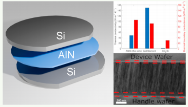
Group II samples were etched from the side of the device wafer and were used to measure the TBC of the deposition interface (TBCAlN/Si, deposition). As illustrated in Figure 1a, the sample consists of layers including the Al transducer, the AlN film (nucleation layer toward the Si substrate), and the deposition interface between AlN/Si and the Si substrate. Illustrations of the samples and a TEM image of the bonded structure before Si etching are shown in Figure 1. The interfaces to be studied were exposed by etching the silicon on the opposing side due to difficulties associated in controlling the silicon etching rate to create a <1 μm thick Si layer after etching 320 μm of Si.

Fig1
Results for the thermal conductivity and TBCs of the bonded AlN samples are given in Table 1. TBCAl/AlN measured in this work is considerably higher than that previously reported by Xu et al.8 and slightly higher than what was reported by Stevens et al.The measured TBCAl/AlN for group II is very close to the TBC calculated using a diffuse mismatch model (DMM);30 however, TBCAl/AlN measured for group I is roughly 20% lower. This is unexpected since picosecond pulses, shown in Figure 2c, seen from both interfaces are identical, which means that the acoustic impedance of the interfaces is similar. Because of this, it seems probable that the AlON interlayer was removed during the Si etching process and does not contribute to the TBC. A possible explanation for the difference in TBC is the existence of the nucleation layer, which can be seen in Figure 1c. The fact that the Al transducer of the group I samples is deposited on top of the nucleation layer, which has greater disorder than crystalline AlN, the TBCAl/AlN for the group I samples can be excepted to be worse than TBCAl/AlN for group II, where the Al transducer is deposited over crystalline AlN.

Fig2
It has been shown that the bonding strength of an interface has a large impact on the TBC, and as such, several works have reported an increase in the TBC when using intermediate layers or even increased surface roughness to increase the bonding strength of an interface. The same phenomena have been demonstrated on bonded GaN samples,where GaN was bonded to various substrates with the help of different intermediate layers to enhance the bonding between GaN and the substrate. Waller et al. studied the necessity of a SiN interlayer for GaN-on-diamond bonding and discovered that the bond that was created through van der Waals bonding had a seven times lower TBC than bonds using a SiN interlayer to facilitate the creation of strong atomic bonds. Furthermore, Cheng et al. showed that an interlayer can reduce the TBC for a GaN/diamond interface, when a thick Si interlayer exhibited a significantly reduced TBC when compared to a thinner amorphous diamond interlayer.
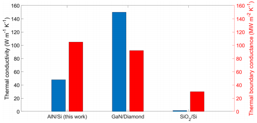
However, the exact mechanism of thermal conduction is not clear. A likely explanation is the extremely high-quality bonded interface, where the only distinct interface observed was between Si and SiO2, which can be seen in Figure 3b. This enables phonon transmission from AlN to Si without significant scattering from the SiO2−AlON interlayer. Lack of a clear interface inside the interlayer is a major difference between the samples measured in this work and samples measured by Cheng at al.,suggesting that an increase in interlayer thickness does not significantly affect the TBC of the interface if the quality of the interlayer remains good. These results indicate that bonded AlN provides a significant improvement over the thermal conductivity of SiO2 and has a TBC comparable to that of GaN. Comparison of thermal conductivity and TBC of AlN, SiO2, and GaN is provided in Figure 4. It should be noted that the AlN used in this work was sputtered AlN rather than MOCVD AlN, which has been demonstrated to have a significantly higher thermal conductivity. Replacing sputtered AlN with MOCVD AlN would increase the thermal conductivity of the AlN and lead to improvements in the TBC between AlN and Si by improving the crystal quality of AlN near the interface.

Fig4
This work studied the TBC of a directly bonded AlN-SOI structure. A 10 nm thick amorphous SiO2−AlON interlayer was created in the AlN-SOI inadvertently during the bonding process as a result of AlN and Si surface activation using SF6 + O2 and SF6 + Ar plasma. Thick amorphous layers, such as these, typically have a very low thermal conductivity and thus need to be characterized thoroughly when attempting to fabricate highly thermally conductive structures. The thermal properties of the AlN-SOI were characterized using TDTR, which showed AlN thermal conductivity at 40−48 W m−1 K −1 and the TBCs between AlN and Si as TBCAlN/Si, deposition = 95 MW m−2 K −1 and TBCAlN/Si, bonded = 105 MW m−2 K −1 . These values for AlN thermal conductivity and the TBCAlN/Si are in good agreement with previously reported values. The results show that AlN-to-silicon direct bonding utilizing plasma activation is a viable method for creating highly thermally conductive SOI structures. This work demonstrates the viability of the AlN-SOI structure as a future platform for high thermal conductivity structures. Future work on the topic should be focused on implementing highly thermally conductive AlN in the AlN-SOI structure to further improve its thermal properties. In addition, devices should be fabricated utilizing the AlN-SOI structure to characterize the functional improvements it provides over traditional SOI.