ABSTRACT
The effect of natural electrode contamination on interfacial energetic, structure and morphology of 𝜋- conjugated organic molecular layers were studied by depositing dinapthothienothiophene (DNTT) thin films of varying thickness on indium-tin-oxide (ITO) substrates and by using photoelectron spectroscopy, atomic force microscopy and X-ray reflectivity techniques. The DNTT thin film on unclean-ITO surface shows a smaller threshold ionization potential (by ∼0.4 eV) compared to the film on clean-ITO one. A molecule–substrate interaction, present in the DNTT/clean-ITO system, gives rise to an interfacial dipole and charge transfer, presumably through flat-lying seed-layer at the interface. On further deposition, the interfacial coverage increases, while the molecules on top of the seed-layer take different orientation (mostly edge-on) to form highly-dewetted fibrous-islands of very high-thickness but very low-coverage. Overall, the growth of DNTT film on clean-ITO surface is layer-plus-island-like or Stranski–Krastanov-type. On the other hand, the contamination layer at the DNTT/unclean-ITO interface is found to act as a spacer layer, which reduces the intimate molecule– substrate interaction and also the roughness to give rise an edge-on ordered island-like or Volmer–Weber-type film-growth with reduced hole injection barrier (by ∼0.2 eV) and better (almost double) film-coverage to make it a more efficient hole injector compared to the clean interface one.
1. Introduction
Continuous development and improvement of organic semiconductor (OSC) based devices, such as organic photovoltaics (OPV) , organic light-emitting diodes, and organic thin film transistors (OTFT), in last few years, have intensified the need to understand the metal electrode–organic interfaces as the performances of such devices strongly depend on the efficiency of charge injection from an electrode into the active OSC material. In OSC-based devices, where transparent electrode is essential, indium tin oxide (ITO) is the natural choice, as it shows very high electrical conductivity (similar to metal) and optical transparency (> 80% in the visible region) . Several studies have been carried out on the interface between ITO and different OSCs to get control over the energy level alignment (ELA) at the interface. However, the role of the natural surface contamination, which can take place due to the exposure of organic thin films or the patterned electrode surfaces into the ambient or poor vacuum conditions prior to the device fabrication, on the ELA at OSC/ITO interface has not been studied so far. A contamination layer, consisting of N2 , O2 , H2O, and hydrocarbons, generally formed on the electrode surface under such exposer, which can not only tune the ELA at OSC/electrode interface but also the conformation and orientation of the molecule and the top surface morphology of the thin film. Hence it is important to study the differences in the OSC/ITO interface energetics made by this unavoidable environmental contamination.
Here, this issue has been addressed by studying the electronic structures of DNTT thin film of varying thickness (from sub-monolayer to multilayer) on unclean and clean ITO substrates using in situ ultraviolet and X-ray photoelectron spectroscopic (UPS and XPS) techniques and subsequently studying the surface morphology of few selected films using atomic force microscopic (AFM) technique. Indeed, the present study shows a noticeable effect of environmental contamination on the electronic structure and morphology of DNTT thin film on ITO. In fact, the adventitious contamination layer present on the ITO surface was found to act as a spacer layer between the ITO surface and DNTT molecular layer, which changes the intimate molecule–electrode interaction to affect the interfacial dipole formation mechanism as well as the ELA and the morphology. The unclean ITO surface, having lower work function, shows closer highest occupied molecular orbital (HOMO) level w.r.t. the Fermi level, lower threshold ionization potential (IPth) and better coverage of the DNTT film compared to those on the clean ITO surface. The possible reasons of such result and its implications on the device performances are discussed.
The electronic structures of the DNTT/ITO interfaces, with or without environmental contamination layer, were characterized systematically by using photoelectron spectroscopic techniques inside an ultrahigh vacuum (UHV) chamber (Omicron Nanotechnology, of base pressure 1.5×10⁻⁹ mbar). The UHV chamber was equipped with an EA125 hemispherical energy analyzer and two monochromatic photon sources. A He gas discharge lamp having photon energy, E0 = 21.2 eV (He I) was used as a UV light source to get the UPS spectra, where the spectrometer energy resolution was ∼0.1 eV. A sample bias of −8.0 V was applied during UPS measurements to determine the higher binding energy cut-off (HBEC). A monochromatic Al K𝛼 (of 𝐸0 = 1486.6 eV) was used as X-ray source for XPS measurements, where the corresponding spectrometer resolution was ∼0.8 eV. All the UPS and XPS spectra were collected keeping the sample at room temperature.
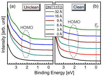
The HOMO region of the UPS spectra for the DNTT thin films of different 𝐷CN-values on unclean and clean-ITO substrates are shown in Fig. 1. The presence of DNTT-related HOMO peak, close to the Fermi level (𝐸F ), though weak due to the higher substrate background signals, is evident in Fig. 1. To get a clear view about the HOMO level, the substrate background subtracted and intensity normalized spectra for the DNTT thin films on ITO substrates are shown in Fig. 2. An increase in the HOMO peak intensity with the increase in the film thickness (as expected) is clearly evident for the DNTT films on both the substrates. The HOMO peak position remains unchanged for the films on the unclean-ITO substrate, whereas a shifting tendency towards the lower binding energy is observed for the films on clean-ITO substrate with the increase of film thickness. For the latter, a small shift of around −0.1 eV is evident for the 32 Å film compared to the 3 Å film. The hole injection barrier height (𝜙Bh), defined as the energy difference between the onset of the HOMO level and 𝐸𝐹 , is found higher for the thin film on the clean-ITO substrate (∼1.7 eV) compared to that on the unclean one (∼1.5 eV), which can be correlated with the different structures of the molecules near the interface arising from different interaction. 𝜙Bh remains almost unchanged for further deposition on the unclean-ITO substrate but decreases for further deposition on cleanITO substrate. Around 0.1 eV shift, towards lower binding energy, was observed for the 32 Å film compared to the 3 Å film. This change in the 𝜙Bh value is an indication in the change of the molecular structure along thickness. Essentially the HOMO region results indicate that the structure of the molecules on unclean-ITO substrate remains unchanged with film thickness, while on clean-ITO substrate, the structure near the interface is different from the remaining top part of the film. The structure of the molecules on top part resembles more to the structure of the molecules on the unclean-ITO substrate.

Fig. 1.
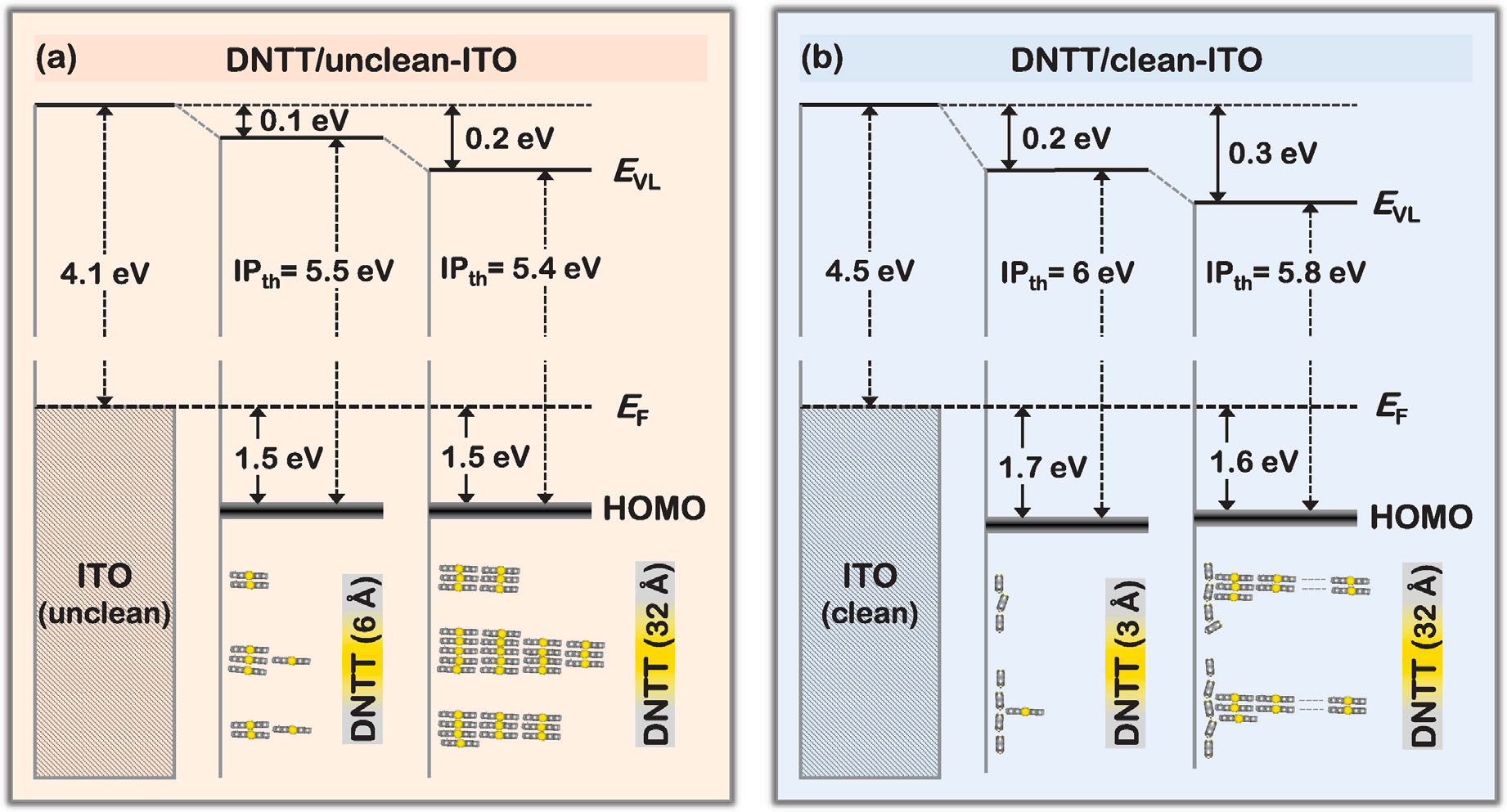
The energy-level diagrams of the DNTT thin films of different thickness on unclean and clean-ITO surfaces and the possible configuration, organization and coverage of the DNTT molecules at the interface and above, as modeled using the information obtained from the complementary UPS, XPS, AFM, and XR techniques and some analogy found in the literature, are shown schematically in Fig. 8 to visualize the overall picture.

Fig. 8
The interfacial dipoles are very influential for the ELA. A large interfacial dipole generally increases the distance between the Fermi level and the onset of HOMO band, i.e. the Bh-value. This is observed in case of DNTT/clean-ITO interface (Fig. 8(b)), where the value of Bh is found around 1.7 eV. The weaker interfacial dipole decreases the Bh-value, which is (1.5 eV) observed for the DNTT/unclean-ITO interface (see Fig. 8(a)). Another important parameter, relevant to the ELA at the interface, is the IPth. This also got affected by the substrate contamination layer. Accordingly, the IPth-value of the unclean-ITO substrate is found less (~0.4 eV) compared to the clean-ITO one and such difference is almost maintained even after DNTT deposition (see Fig. 8).
In conclusion, the effect of substrate contamination on the ELA at the DNTT/ITO interface and also on the thin film growth mechanism were studied systematically. The contamination layer on the ITO surface partially suppresses the surface component of electron wave function, which normally tails into the vacuum at the ITO surface, to reduce the work function of the ITO surface, resulting in a less reactive interface. This layer also found to prevent the intimate organic–electrode interaction, which dominates at the clean interface causing a higher hole injection barrier that is a very important parameter in the context of charge transport in the device structure of organic semiconductors. According to the IDIS model, the less intimate contact between organic molecule and electrode substantially reduces the density of states around CNL of the organic molecules, resulting in a weaker pinning of the Fermi level around CNL and, consequently, the interface energetics is much closer to the vacuum-level alignment (Fig. 8) . In the present case, the contaminated ITO substrate with lower work function gives a weaker interfacial dipoles, resulting in a smaller Bh as compared to the clean interface and also an IPth which is close to the value of bulk DNTT and comparably lower (around 0.4 eV) than the DNTT on clean surface. The crystallinity of the DNTT film is found higher for the unclean surface where the film coverage is better than that on the clean surface. Overall, the electronic structure and thin film structure of DNTT molecules on ITO substrate are found to influence by the interface cleanliness, which are of immense importance for controlling the performances of the organic semiconductor-based devices.
上一篇: 直接键合氮化铝与硅界面的热边界导率
下一篇: 4H– SiC功率器件的击穿电压能力