ABSTRACT
Power semiconductor devices are constructed to endure high voltages (>30 V) and manage high current density. Edge termination is a specific feature that must be integrated into the device architecture to achieve high voltage capability in vertical power components. It is necessary to design these edge terminations while taking into account the device’s architecture and technology. Termination efficiency is the main factor, but its area is also of great significance. Many edge termination designs with efficiency close to 100 % have been reported and are currently used in commercial devices. However, having a near-100 % static breakdown voltage is not the only requirement in modern power devices. Today, most power applications rely on the avalanche capability as a key parameter. Avalanche capability is defined by the device ability to enter in non-destructive avalanche mode, where the component can temporarily sustain a high voltage and a high current in blocking mode. The Unclamped Inductive Switching (UIS) test can be used to measure the avalanche mode, and it can be customized to define a safe operating area for a full avalanche mode (SOA). The safe operation of both single pulse and repetitive pulsed avalanche limits can be characterized. Such operation mode is now controlled in both Silicon and Silicon Carbide based power devices. However, the development of novel wide and ultra-wide band gap semiconductors in regards to avalanche capability and SOA still require a lot of work.
1. Introduction
Electrification is one of the most important strategies for driving the transition from fossil fuel to renewable energy. Power electronics form a crucial part of this transition. In fact, power devices are semiconductor-based architectures able to manage high voltage and/or high current for conditioning electrical energy. They are used in almost all the electronic systems and applications, usually to control the energy supply to the electronic systems or to electrical loads (motors, actuators …). Power electronics use these devices in different family of circuits such as rectifiers, converters or breakers. Typically, the semiconductor power devices can suffer from electrical parasitic’s such as overvoltage or surge energy generated by the load or the power circuit. Consequently, the design of such components must be robust and take into account safety margins defined in the so-called Safe Operating Areas (SOA).
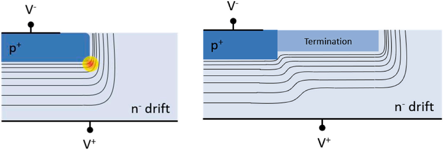
Two primary architectures are used for power semiconductor devices: lateral and vertical, depending on the direction of dominant current flow . A schematic illustration of these architectures is represented in Fig. 1. In lateral devices, the current flows laterally between two electrodes located on the surface of the semiconductor, like many other semiconductor devices such as CMOS circuits. The vertical architecture results in current flowing from the top to the bottom of the semiconductor die, between two electrodes on either side. In both architecture configurations, the component’s maximum voltage capability requires the addition of specific features to the device structure. In a vertical device, this feature is called edge termination and is located at the periphery (see Fig. 2.) of the active area driving the current.

Fig. 1

Fig. 2
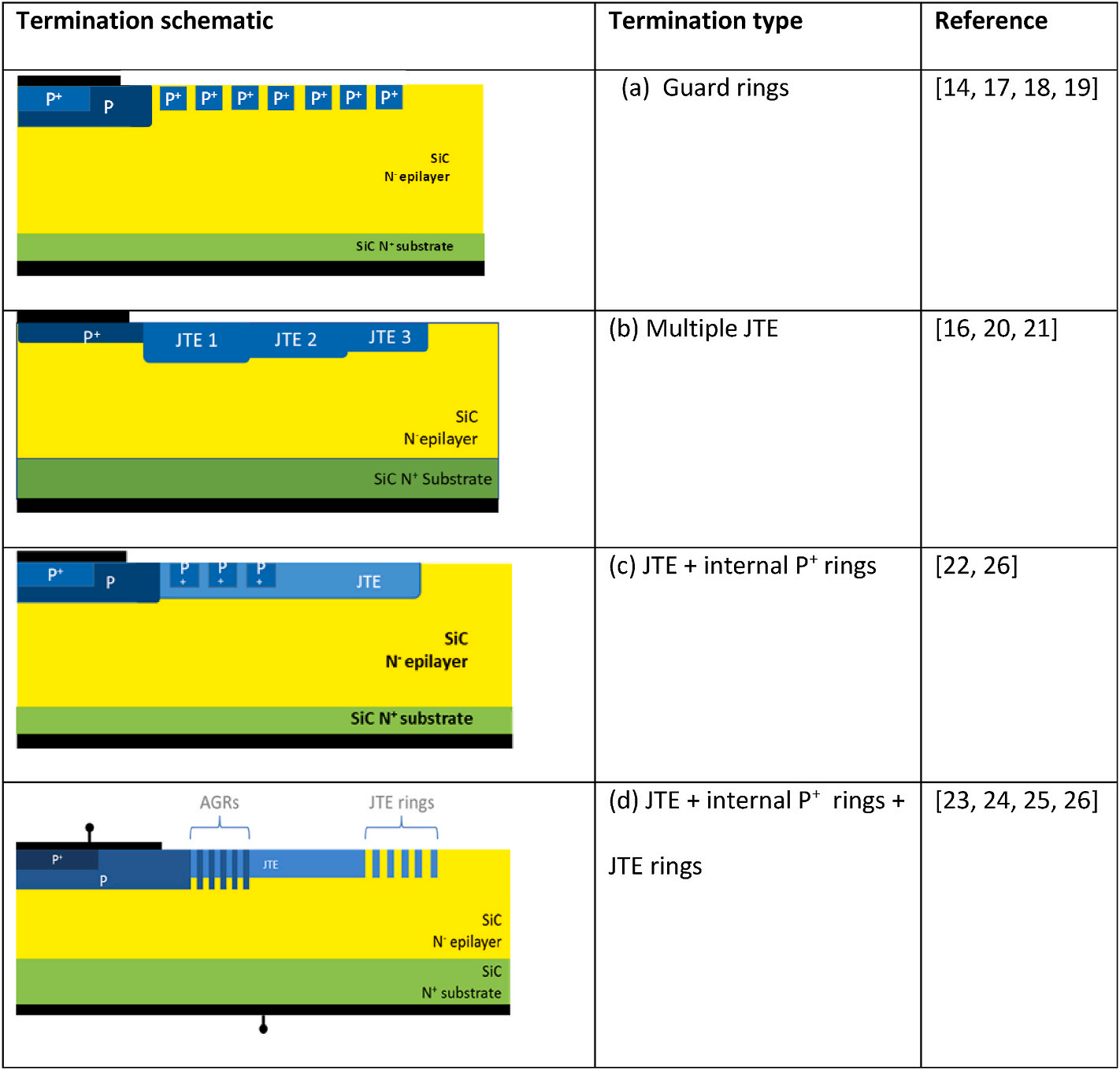
The edge termination of most recent vertical power devices in Si or SiC is achieved by using selective P doped wells obtained through ion implantation. Usually, these edge terminations are built either with P rings with high doping (>1E19 cm−3 ) or/and with Junction Termination Extension (JTE) with moderate doping (few 1e17 cm− 3 ) . There are numerous and diverse combinations of both structures that have been reported and are currently employed in commercial SiC diodes and transistors. Fig. 1 displays a non-complete list of suggested architectures. Pure P+ rings edge termination (Fig. 3a) is advantageous because nearly all power devices have implanted P+ profiles in their active cell process flow. This simplifies the fabrication process and reduces costs by eliminating the need for extra photolithography or p-type implantation steps to implement the termination. However, this ring termination requires meticulous control of the photolithography dimensions, particularly regarding the first ring position, and typically takes up a large area (>20 rings). The JTE structure (Fig. 3b) necessitates an additional mask level and implantation step, but when combined with internal or external rings, it leads to optimal efficiency and a shorter termination length. In power MOSFETs, a deep P-body is implanted to form the channel area. One may consider to use this implant to form an edge termination. However, up to now, tentative to use this P-body layer as JTE failed due to a higher p-doping than the optimal one. Therefore, it is necessary to perform a specific Al implantation step or multiple mask levels etching of the P-body (Fig. 3i) as required. A gradual lateral doping along the x-axis is highly beneficial for efficient termination in the JTE design. In silicon, it can be done by opening variable width implantation windows and playing with the lateral diffusion of the dopants during thermal treatment. In SiC, dopants do not diffuse at reasonable temperatures (<1800 ℃). An alternative technique to obtain lateral doping variation of the JTE is to combine the single implantation step with multiple etching steps as proposed in Ref. and shown in Fig. 3f.

Fig. 3
Therefore, it may be possible to incorporate a partial trench etching at a technologically realistic depth with P+ rings implanted at the bottom of the trench, as described in Refs. . In this case, the trench does not need to reach the N+ buffer below the drift region. By utilizing conventional ion implant and SiC etching processes, devices with higher voltage ranges can be made.
Cosmic rays are high radiation energy particles that can lead to spontaneous failures in semiconductor devices biased in blocking mode or under high electric field. The impact of cosmic rays on power semiconductor component for terrestrial applications have been shown first for Silicon devices . The underlying mechanism for failure of power device have been identified as massive charge multiplication triggered by a nucleon-nucleus collision that creates an energetic recoil. Similarly to Si, in high electric field regions of SiC devices, the strong avalanche charge carrier multiplication is sufficient for causing single event burnout . In terrestrial applications, these particles are typically neutrons and their flux exponentially increase with the altitude. In Si, mitigation is done through specific design allowing a reduction of the electric field peaks at the p/n junctions, or using a voltage range derating. In SiC, involved electric fields are usually 10 times higher. However, this is mitigated by a thinner drift layer and a smaller die area for a given voltage capability and nominal current. It helps to reduce the probability of a collision with a particle. Indeed, experimental results show a higher robustness of SiC devices versus their Si counterparts.
Solid-state SiC power devices with breakdown voltages of up to 15 kV can be regularly demonstrated using the established design guidelines and technology procedures for active and edge termination zones. High breakdown effectiveness is the main reason for the widespread use of terminations that are based on guard rings or JTE with rings. Certainly, the majority of commercial SiC devices are designed to withstand avalanches. Single pulse avalanche current easily reaches the nominal forward DC current ratings, while repetitive avalanche mode is also possible with very low performance’s drift. These avalanche modes capabilities are required in most modern power circuit applications where inductive loads and parasitic interconnection inductances are present. The measurement of avalanche capability directly on-wafer is not straightforward, as misunderstandings are possible when analyzing a static I–V curve. Then, either temperature-dependent measurement on wafers or dynamic tests (UIS) on packaged devices are required. UIS test results may be influenced by the transient dV/dt rates applied to the device under test. UIS test standards have been developed for Si devices, with operation frequencies in the 10th of kHz range. However, new power semiconductors such as SiC and GaN operate at higher frequencies. Then, high frequency pulse tests may be necessary to emulate the operating conditions of the novel power application.
下一篇: 3C-碳化硅-铌酸锂集成光子平台