Abstract: In this paper, we demonstrate a novel hybrid 3C-silicon carbide-lithium niobate (3C-SiC-LN) platform for passive and active integrated nanophotonic devices enabled through wafer bonding. These devices are fabricated by etching the SiC layer, with the hybrid optical mode power distributed between SiC and LN layers through a taper design. We present a racetrack resonator-based electro-optic (EO) phase shifter where the resonator is fabricated in SiC while using LN for EO-effect (r33≈ 27 pm/V). The proposed phase shifter demonstrates efficient resonance wavelength tuning with low voltage-length product (Vπ.Lπ ≈ 2.18 V cm) using the EO effect of LN. This hybrid SiC-LN platform would enable high-speed, low-power, and miniaturized photonic devices (e.g., modulators, switches, filters) operable over a broad range of wavelengths (visible to infrared) with applications in both classical and quantum nanophotonics.
1. Introduction
Integrated photonic material portfolio has been recently extended to the likes of silicon carbide (SiC) and lithium niobate (LN) owing to their unique material properties for both classical and quantum photonics. SiC has a broad transparency range (wavelength: 0.37-5.6 µm) and exhibits a wide range of nonlinear optical effects. SiC exists predominantly in three polytypes: 3C (cubic), 4 H and 6 H (hexagonal). 4H-SiC is available in thick bulk crystalline form and is converted into 4H-SiC-on-insulator (4H-SiCOI) using ion-implantation, bonding, and etching to form a thin (thickness ∼ 600 nm) SiC layer to enable photonic device fabrication. Alternately, 4H-SiCOI prepared from oxide-fusion bonding and rigorous polishing (to thin down the thick SiC layer to the desired thickness for device operation) has been widely used for microelectromechanical systems (MEMS). A similar approach adopted for photonics, avoids the crystal-damage arising from ion-implantation thereby enabling high-quality resonators and photonic crystal cavities for nonlinear applications.
2. Hybrid SiC-LN integrated photonic platform
We begin the process with a 4” 3C-SiC and an X-cut LNOI wafer. The 3C-SiC (from NovaSiCTM) is formed by epitaxial deposition of a 2 µm-thick layer of SiC over a 510 µm-thick Si substrate followed by a chemical-mechanical-polish (CMP) step. The thin-film LN wafer (from NANOLNTM) consists of a ∼ 270 nm-thick X-cut LN layer on a 4.7 µm buried-silicon oxide (SiO2) layer over a Si substrate (thickness ∼ 525 µm). First, these wafers are thoroughly cleaned using the standard SC-1 (5:1:1 volume ratio of H2O, NH4OH, and H2O2), and SC-2 (5:1:1 volume ratio of H2O, HCl, and H2O2) solutions, followed by the deposition of a 45 nm-thick SiO2 layer through atomic layer deposition (ALD).
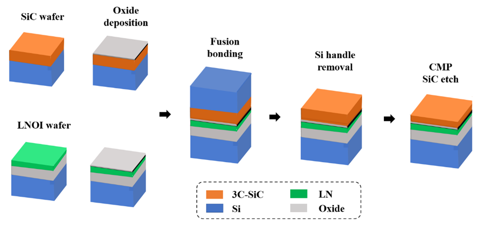
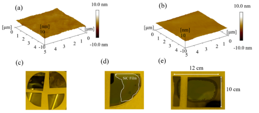
The process flow for the wafer bonding is illustrated in Fig. 1. We perform a direct fusion bonding of the SiC and LNOI wafers, with the thin interface oxide where the hydrophilic bonds are created. Typically, these bonds are strengthened during the high-temperature annealing process. However, the CTE values for SiC (2.7 × 10⁻⁶ K −1 ) and LN (13.4 × 10⁻⁶ K −1 along the X and Y axes) are widely different even at room temperature. This difference aggravates at higher temperatures and leads to wafer cracking due to thermal stress. Stronger surface activation could enable low-temperature bonding without compromising the bond strength. In our approach, we treat the wafers with de-ionized water before placing them in a chamber with high vacuum under nitrogen plasma to increase the hydrophilicity of the wafer surfaces [30]. The AFM measurements for the SiC and LNOI wafers before bonding are shown in Figs. 2(a) and (b), respectively. We can see that the wafer surfaces prior to bonding are smooth with root-mean-squared (RMS) roughness (σ) < 1 nm. After activation, the wafers are pre-bonded at room temperature under a force of 2 kN followed by annealing at a temperature of 100 oC over 20 hours to increase the bond strength. The bonded wafer pair is cleaved into four quarters (Fig. 2(c)), and the post-processed quarter is depicted in Fig. 2(d) showing the bonded 3C-SiC film over LN. This die is further processed by removing the Si handle layer and CMP to thin down the SiC film to 280 nm, and the final cleaved die is shown in Fig. 2(e).

Fig1

Fig2
The Si handle removal during post-processing consists of dry etching in SF6 (sulfur hexafluoride) plasma, followed by wet etching in a 45% KOH (potassium hydroxide) solution for several hours. The surface of the SiC film after the Si-removal contains residues that lead to a rough surface as seen from the AFM measurement shown in Fig. 3(a). This final surface is polished-off in a chemical-mechanical-polishing (CMP) step. As shown in Fig. 3(b), the surface roughness is considerably improved after CMP, which removes the surface residues and the defects at the SiC/Si layer. The cross-sections of the bonded samples after Si-handle removal and after further CMP are depicted in the scanning-electron-microscopy (SEM) images of Figs. 3(c) and 3(d), respectively.

Fig. 3
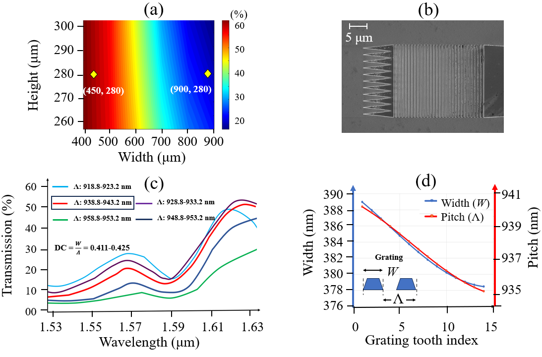
First, we performed Lumerical simulations to arrive at the optimal waveguide dimensions tosupport a single mode operation while considering the film thickness variations (as waveguideheight). We selected the width of the waveguide to be ~900 nm to provide single-mode operationand to maintain relative power distribution between SiC and LN layers. For the resonator, thebend radius is chosen to accommodate low bend loss (see Supplement 1 for details). Note thatthis number might change through a rigorous multi-scale optimization of the overall device infuture, but it is a good choice for an initial demonstration. The waveguide width also influences the mode distribution in the SiC and IN layers. Figure 4(a) shows the confinement (9 of electricfield intensity in LN) distribution map of the fundamental transverse-electric (TE) mode withelectric field in the plane of the waveguide, for different waveguide dimensions. To couplethe light into and out of the integrated photonic chip, multiple eficient apodized grating GCs(Fig. 4(b)) are designed considering the process and SiC thickness variations. The simulatedtransmission spectra for different GC's are shown in Fig. 4(c), which indicate high transmissioneficiency up to 50% or above thereby ensuring significant fiber-grating optical coupling afterdevice fabrication. Figure 4(d) shows the apodization of tooth width and pitch for one of the GCs.

Fig4
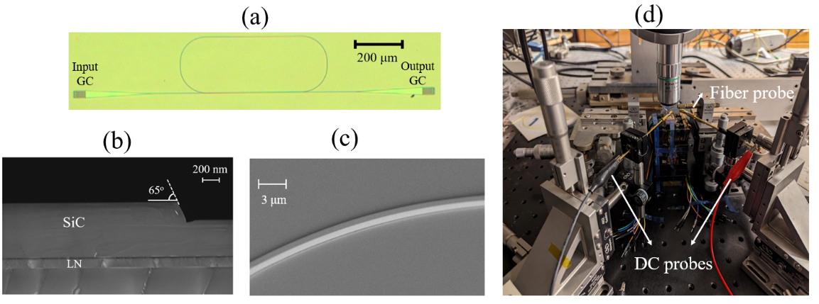
Figure 5(a) shows a racetrack resonator with input/output GCs which is further integrated with electrodes. On these devices, we observed a side wall angle of 65o (Fig. 5(b)) with smooth sidewalls (Fig. 5(c)). The metal electrodes are fabricated for the application of the DC electric field to the LN layer for active (EO) tuning of the device response. For the electrode-fabrication, we spin-coat a 770 nm-thick layer of PMMA (A6) as the electron-beam (e-beam) resist, patterned by electron-beam lithography. This is followed by the development, metal deposition (300 nm gold (Au) /20 nm of titanium (Ti)) using e-beam evaporation and a final lift-off in acetone to form the electrodes. characterized using the experimental set up shown in Fig. 5(d) with input-output cleaved fibers for light coupling into the gratings. The DC probes are arranged to supply the DC voltage to the fabricated Au electrodes.

Fig. 5
In summary, we demonstrated here a novel hybrid 3C-SiC-LN platform where CMOS compatible fabrication is conducted on the SiC layer, and the bonded LN layer provides the EO effect for tuning. On this platform, we demonstrated an EO phase shifter integrated into a racetrack resonator providing a low Vπ.Lπ ≈ 2.18 V cm. The combination of the high-speed and energy-efficient EO effect in LN with the broad wavelength transparency and CMOS compatibility features of SiC will enable broadband high-speed devices (e.g., modulators and switches) with low-energy consumption fabricated in a CMOS compatible process flow. While this paper demonstrates the feasibility of this unique platform, future research for improving the performance measures and material quality will be needed to convert it into a universal CMOS-compatible platform for ultrafast, low-power, and miniaturized nanophotonic systems for passive, active, nonlinear, and quantum photonic applications.