Abstract: To address surface morphological defects that have a destructive effect on the epitaxial wafer from the aspect of 4H-SiC epitaxial growth, this study thoroughly examined many key factors that affect the density of defects in 4H-SiC epitaxial wafer, including the ratio of carbon to silicon, growth time, application of a buffer layer, hydrogen etching and other process parameters. Through systematic experimental verification and data analysis, it was verified that when the carbon–silicon ratio was accurately controlled at 0.72, the density of defects in the epitaxial wafer was the lowest, and its surface flatness showed the best state. In addition, it was found that the growth of the buffer layer under specific conditions could effectively reduce defects, especially surface morphology defects. This provides a new idea and method for improving the surface quality of epitaxial wafers. At the same time, we also studied the influence of hydrogen etching on the quality of epitaxial wafers. The experimental results show that proper hydrogen etching can optimize surface quality, but excessive etching may lead to the exposure of substrate defects. Therefore, it is necessary to carefully control the conditions of hydrogen etching in practical applications to avoid adverse effects. These findings have important guiding significance for optimizing the quality of epitaxial wafers.
1. Introduction
With the gradual advancement of silicon carbide (SiC) chemical vapor deposition (CVD) technology, the SiC growth process has approached maturity, and the primary obstacle to producing SiC semiconductor epitaxial wafers lie in the presence of epitaxial defects. These defects pose significant challenges for high-voltage and high-power SiC power electronic devices. The origins of these defects are often related to many factors, such as substrate quality, growth temperature and cavity structure, and the crystal structure of these defects is usually complicated. High-voltage and high-power SiC power electronic devices need a large active area to realize high-current applications. Defects in the active region degrade the performance of devices and further lead to device failure. Especially, some fatal defects can greatly reduce a device’s breakdown voltage and may cause long-term reliability problems.
The epitaxial defects of silicon carbide are mainly divided into surface morphology defects and internal structure defects, and internal structure defects are mainly dislocation and some hole-like point defects. Micropipes in structural defects cause serious damage, but they have already been solved. Other structural defects, such as through edge dislocation (TED) and through screw dislocation (TSD), cause surface pits and increase leakage current, which are less destructive. The main destructive defects are instant surface dislocation (BPD) defects and stacking faults (SF), which are likely to continuously increasethe on-resistance of bipolar devices. Surface defects, such as dump, scratch, particledownfall (DF), triangle (TD), comet and carrt defects, are typically detrimental and easilyobservable,and often lead to device failure.
2. Experimental
To determine the influence of some prcess parameters on the density of defects, weused a 4° inclination angle to grow a 6-inch 4H silicon carbide epitaxial wafer. Trichlorosilane (TCS, SiHCl;) was used as the silicon source. TCS ensured that the ratio of siliconto chlorine was 1/3, ethylene was used as the carbon source, hydrogen was used as thecarrier gas, and the ratio of silicon to hydrogen was 0.05%, which is around 50 sccm TCSand 100 slm H,. The conventional conditions were a C/Si ratio of 0.72, temperature olabout 1570 'C, pressure of 40 torr, and epitaxial growth for 30 min. The experimentaconditions of the target test items were adjusted, while ensuring that other experimentalconditions remained unchanged. SICA examination equipment for distinguishing defectsusing photoluminescence defect morphology was used to detect and count the densityof defects to investigate how the density of defects changes under different conditionsThe main defects found using this examination are presented in Figure 1. Among themdefects with PL preceding the defect name are those that have not been found under ordinary optical inspection, but only found under photoluminescence examination. P..whiteand PL,.black are defects such as TED and TSD, and this examination method could notaccurately distinguish between these two defects.
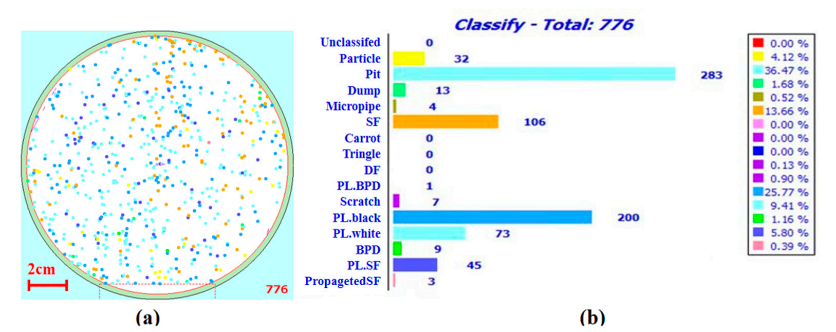
Fig 1
3. Results
Through comparative experiments, the effects of process parameters, such as the C/Si ratio, temperature, growth time, buffer layer and etching conditions, on the density of epitaxial defects of 4H-SiC were identified. A scanning electron microscope (SEM) provides high-resolution images of the surface topography and can be used to analyze the morphology, composition, and crystal structure of materials. The surface of the grown epitaxial wafer was observed by SEM, and the main defects observed are shown in Figure 2. The two defect types are comet defects and triangle defects; comet defects are caused by downfall defects, while triangle defects may be caused by structural defects inherited from the substrate in addition to dropouts.
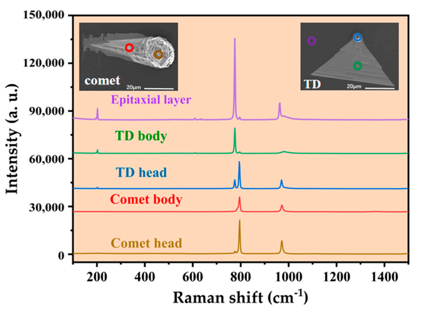
Fig2
Figure 2 shows the Raman examination of two common surface defects. The one witha peak at 777 cm1 is a 4H crystal form, and the one with a high peak at 798 cm-1 is a 3Ccrystal form. Therefore, the head and body of comet defects were both the second phase ofthe 3C structure, the head of triangular defects was a mixed crystal form dominated by a3C structure, and the body parts were all 4H crystal forms, like epitaxial layers.
In Figure 3a, boxes show the overall situations of defect density under different C/Siratios, which could obtain the density of epitaxial defects under different C/Si ratios, reflectthe discrete nature of defect density data to a certain extent, and obtain the stability olthe defect density under these C/Si ratios, i.e., it was not easy to obtain epitaxial waferswith particularly high defects. The effect of C/Si on roughness is shown in Figure 3b, andthe results for roughness were close to those for defect density. The optimum value wasobtained around C/Si= 0.72, and it can be concluded that the defect density can be bettersuppressed at this C/Si ratio. According to the analysis ofobtained data, the defect densitydid not increase gradually with the increase in the C/Si ratio, but was obtained when theC/Si ratio was maintained at a low level, and after the C/Si ratio reached the C/Si ratio led to an increase in defect density to some extent. When the C/Si ratio was0.72, the sample with the smallest defect density was obtained. The overall defect densitywas low. On the contrary, samples with a higher defect density than those in the samegrup appeared in the other three grups ofC/Si ratio tests, which may have been causedby the temperature change during the heating process.
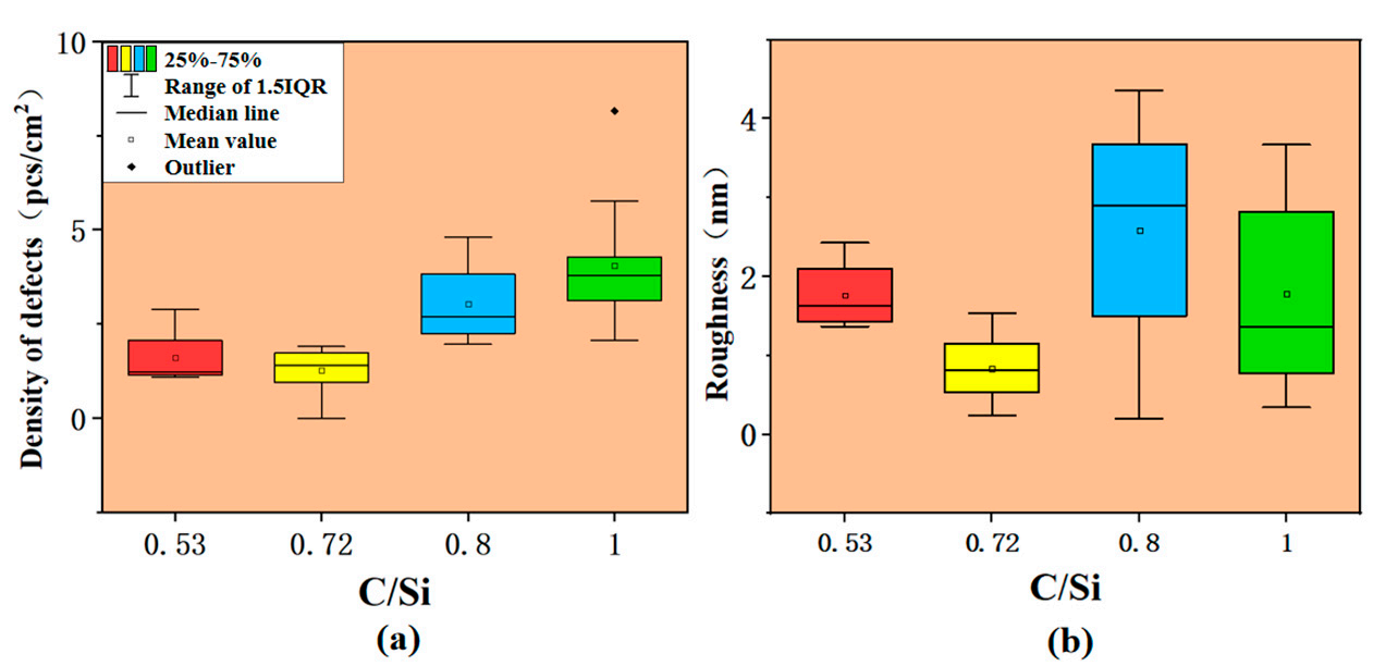
Fig3
Figure 4 shows atomic force microscope (AF) images taken at different C/Si ratiosan AFM was used to test a plane of 10 um x 10 um in tapping mode. Roughness, as shownin Figure 4, was generally used to express the surface quality of epitaxial wafers. Howeverin the same batch of epitaxy, the main reasons for mughness were pits and steps, as shownin the following atomic force images in Figure 4, which seriously increased the surfaceroughness. The pits were formed by BPD defects extending to the epitaxial surface. Whenthe C/Si ratio was 0.72, both the roughness and the density of defects were relatively lowwhich showed that a C /Si ratio of 0.72 is an excellent condition to keep the surface smoothwith fewer defects in process growth.
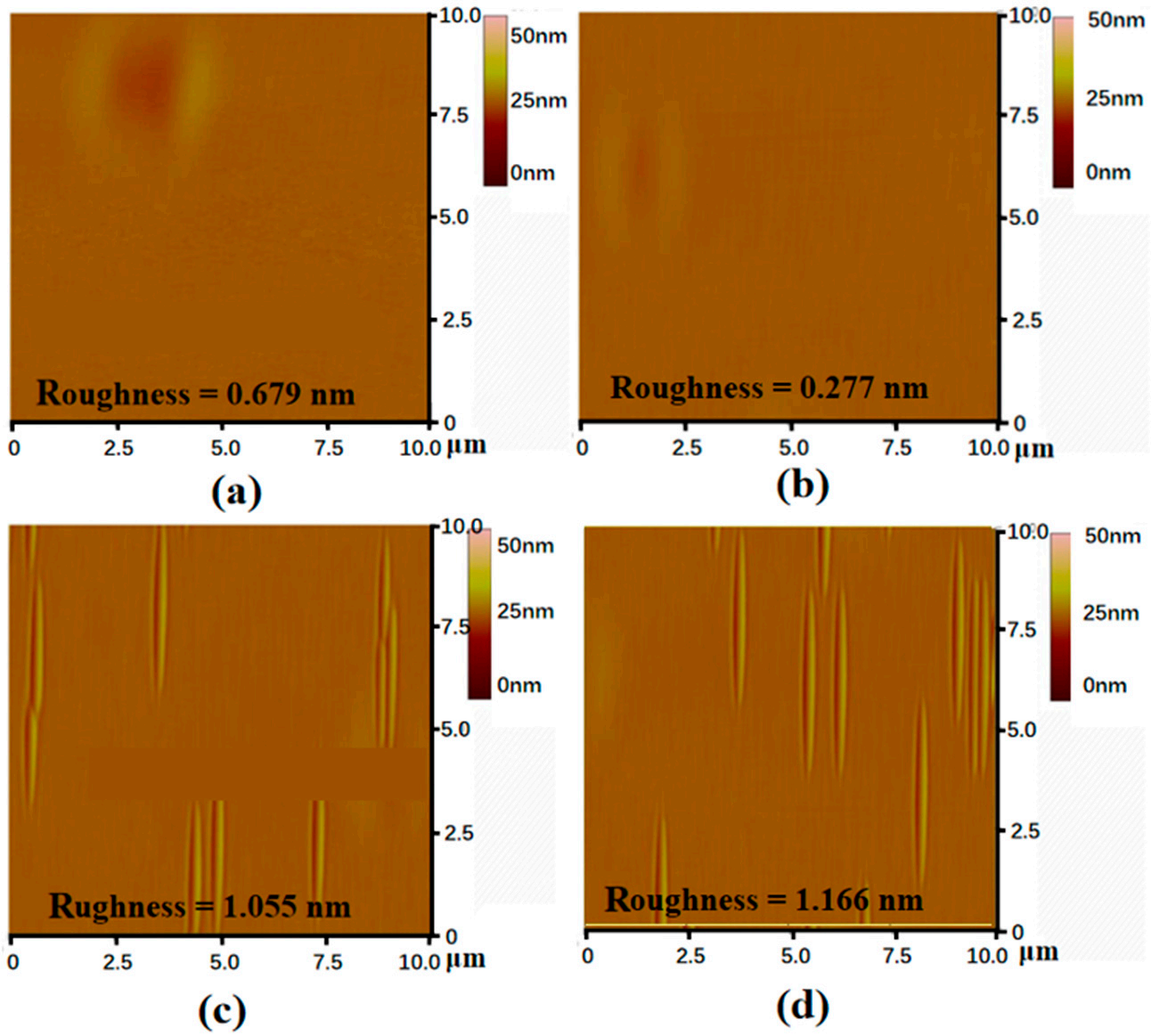
Fig4
The reason for this phenomenon may be that the C/Si ratio was affected by the lelement in the growth source TCS, which hindered the Si elements combining to formsilicon drops during SiC epitaxy. On the other hand, under the condition of rich siliconelement C is also difficult to polymerize into carbon particles, and silicon droplets andcarbon falling particles are the main generation sites of surface defects, which means thatthe higher the C content, the easier it is to prduce defects. We can control the generationof epitaxial defects to some extent by controlling the ratio of carbon to silicon. Aftersubsequent reference to defect types, defect density, defect distribution, surface moughnessroughness distribution uniformity and various tests, we think that when 'TCS is used as aSi source for silicon carbide epitaxial wafers growth, there are fewer defects when the C/Siratio is about 0.72.
It can be observed from Figure 5 that the density of defects decreased when epitaxial growth time increased from 10 min to 25 min, and reached a minimum at 25 min, but when epitaxial growth time was adjusted to 40 min, the density of defects increased abnormally compared with the previous states.
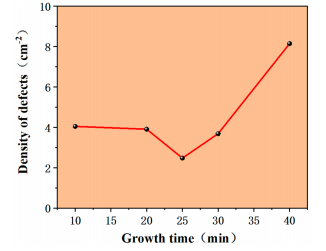
Fig5
The reason for this phenomenon may be that the types of defects were related tothe differences in nucleation methods. In the initial stage of growth, defects were mainlystructural defects inherited from the substrate or surface defects formed with substratedefects as nucleation sites. During the growth pmcess of 10-25 min, some structuraldefects inherited from the substrate gradually decreased due to their own transformationand annihilation mechanisms, until they reached a low level at 25 min, during which thetransformation from BPD to TED occurred, When the epitaxial time continued to increaseto 30 min, the surface morphology defects of downfalls and nucleation of falling particlesmay have become the mainstream of defects. With the continuous accumulation of defectsthe density of defects increased sharply. Therefore, controlling the growth time can be aneffective method to reduce the density ofdefects. This method requires numerous attemptsduring actual prduction, focusing on identifying the lowest density of defects growingwith time, and then devising production plans accordingly.
上一篇: 3C-碳化硅-铌酸锂集成光子平台
下一篇: 单晶 4H-SiC 块体衬底的受控剥落