We detail several scientific and engineering innovations which enable the controlled spalling of 10 – 50 micron thick films of single crystal 4H silicon carbide (4H-SiC) from bulk substrates. 4H-SiC's properties, including high thermal conductivity and a wide bandgap, make it an ideal candidate for high-temperature, high-voltage power electronic devices. Moreover, 4H-SiC has been shown to be an excellent host of solid-state atomic defect qubits for quantum computing and quantum networking. Because 4H-SiC single crystal substrates are expensive (due to long growth times and limited yield), techniques for removal and transfer of bulk-quality films in the tens-of-microns thickness range are highly desirable to allow for substrate reuse and integration of the separated films. In this work we utilize novel approaches for stressor layer thickness control and spalling crack initiation to demonstrate controlled spalling of 4H-SiC, the highest fracture toughness material spalled to date. Additionally, we demonstrate substrate re-use, bonding of the spalled films to carrier substrates, and explore the spin coherence of the spalled films. In preliminary studies we are able to achieve coherent spin control of neutral divacancy (VV0 ) qubit ensembles and measure a quasi-bulk spin T2 of 79.7 µs in such spalled films.
1. Introduction
Controlled spalling of semiconductors is a technique developed for removing thin (10 – 50 micron) layers from atop a semiconductor substrate by triggered and deliberate propagation of a sub-surface crack across the entirety of the chip or wafer.Stress is built up in the wafer subsurface by the deposition of an appropriate metal (stressor) layer on the wafer surface. The crack originates at the wafer edge and then propagates laterally at a depth of 10 – 50 microns to relieve this stress without a need for post-conditioning (e.g. heat treatments). Spall depth can be modulated by engineering the stress field via the metal film deposition. A significant benefit of spalling is that the bulk-like properties of the exfoliated film are preserved[3–5] since the crack depth is determined by an elastic stress field, rather than an intervention by ion implantation or by the deposition of heterogeneous layers at the separation interface. The principal breakthrough in spalling was made by Bedell et al. who introduced a controllable method for spalling using nickel films deposited under high tensile stress via sputtering or electroplating. This method has proven to be highly versatile, and to date has been used to spall Si, Ge, and III-V semiconductor wafers. Silicon wafers of up to 300 mm in diameter have been spalled.However, the materials spalled so far have been semiconductors with moderate to low fracture toughness and there have been no reports of successful spalling of more refractory, hard materials with a significantly higher fracture toughness.
2. Results and Discussion
Prior to spalling, a film of metal (typically Ni) is deposited onto the wafer to be spalled such that stresses in the metal layer give rise to an elastic stress field in the wafer subsurface region.[16] The higher the fracture toughness of the wafer, the higher the thickness and stress of the metal film required to induce steady state spalling. The theoretical model which has proven to be valuable for predicting this thickness and stress is described by Suo and Hutchinson and enables calculation of the stress intensity factors KI and KII of a propagating crack within the substrate. Details and an application of this model have been described by Bedell et al.[4] In summary, the crack originates at a free surface (usually the top surface of the semiconductor wafer) and propagates as a mixed mode crack (non-zero values of KI and KII) plunging into the semiconductor. At a specific depth (predicted by the Suo and Hutchinson model) when KII ~ 0, the crack propagates in a direction that is on average parallel to the surface and spalls off a film of the semiconductor substrate attached to the metal stressor layer.
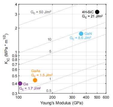
Here, E is the Young’s modulus and ν is the Poisson’s ratio of the crack propagation medium. The semi-log Ashby plot in Figure 1 illustrates the strain energy required for spalling 4H-SiC as compared to various materials which have previously been spalled. GaN was previously the most challenging material that had been spalled, whereas the 4H-SiC spalling demonstrated in this work requires almost 2.5 times more strain energy. The material properties used in this plot were gathered from a breadth of reported data as well as the previous papers on the spalling of each of the materials listed. Figure S1 gives further details on the required Ni metal stressor layers needed for spalling the selected materials. This previously unexplored level of strain energy per unit area applied to the metal-semiconductor spalling system poses new challenges critical to spalling of hard materials, notably (i) the thickness distribution of the metal film and (ii) the spalling crack nucleation. The scientific approaches used to address and overcome these challenges are described in this work and are expected to be applicable to the spalling of many other high fracture toughness semiconductors beyond 4H-SiC. We address below some of the key materials issues relevant to the spalling of such ultra-hard materials.

Fig1
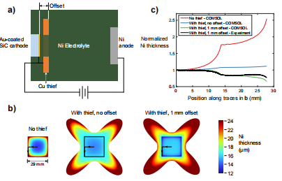
To address the problematic thickness nonuniformity of electroplated Ni, an auxiliary cathode which is known in the electroplating industry as a “thief”[32] was designed and integrated into the electroplating setup. The thief adds additional surface area to the cathode and can be used to control current density at the edges of the target substrate by altering the current distribution. Figure 2a shows a diagram of the electroplating bath with the thief shorted to and coaxially offset from the Au-coated 4H-SiC cathode (which, as note earlier, acts as the seed for electroplating Ni). An iterative design process for the thief utilized finite element modeling in COMSOL to simulate the Ni electroplating thickness profiles on a 29 x 29 mm square substrate (typical size of 4H-SiC die used in this work) as a function of the size, shape, and position of a conductive thief surrounding it. Details of the electroplating parameters used in these simulations are given in the methods section.

Fig2
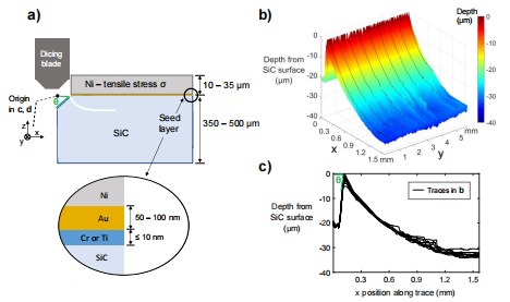
Another concern for the spalling of ultrahard materials is that crack initiation – the prerequisite to steady state spalling – was found to be unreliable when utilizing controlled spalling techniques which have been established previously. The conventional method by which spalling crack initiation is made into Si and other semiconductors of similar toughness is to make the Ni abruptly discontinuous away from the substrate edge. The stress concentration where the edge of the Ni meets the substrate is then high enough such that a crack can initiate either spontaneously when a certain Ni thickness is reached, or with external force from a handle layer of tape which is applied on top of the Ni and pulled upwards. In this case, no modification of the substrate is needed to initiate a spalling crack, i.e. θ = 0° as defined by the diagram in Figure 3a. For 4H-SiC however, we found that crack initiation fails when using this technique. Rather than inducing a spalling crack, the Ni delaminates from the Cr/Au or Ti/Au electroplating seed layer, specifically at the interface between the Au and Ni (see Figure S2).

Fig3
3. Conclusion
Controlled spalling of 4H-SiC has been successfully demonstrated on a wide variety of substrate types and sizes. Reliable spalling of this high fracture toughness material is made possible by innovations in the stressor layer thickness distribution and spalling crack initiation into the 4H-SiC. Thickness nonuniformity across an entire spalled film is currently ~ 6 μm peak-to-peak, limited primarily by further advancements needed in regulation of the peeling process. Intrinsic roughness of 4-degree miscut substrates can be kept under 1 μm peak-topeak by spalling perpendicular to the miscut direction. Heterogenous integration and substrate re-use show promise, with more complicated schemes to be pursued in future work. An initial demonstration of coherent spin control of a VV0 ensemble in spalled 4H-SiC yields a spin T2* which is similar (~ 78%) to the bulk value and a spin T2 which is likewise similar (~ 68%) to the bulk value, sufficient to motivate future exploration of spalled films incorporated with onchip silicon photonics. Other goals for future work include spalling full 150 mm and 200 mm wafers of 4H-SiC as well as exploring the spalling of 4H-SiC substrates with prefabricated power devices on the wafer surface.