ABSTRACT
The combining microelectronic devices and associated technologies onto a single silicon chip poses a substantial challenge. However, in recent years, the area of silicon photonics has experienced remarkable advancements and notable leaps in performance. The performance of silicon on insulator (SOI) based photonic devices, such as fast silicon optical modulators, photonic transceivers, optical filters, etc., have been discussed. This would be a step forward in creating standalone silicon photonic devices, strengthening the possibility of single on-chip nanophotonic integrated circuits. Suppose an integrated silicon photonic chip is designed and fabricated. In that case, it might drastically modify these combined photonic component costs, power consumption, and size, bringing substantial, perhaps revolutionary, changes to the next-generation communications sector. Yet, the monolithic integration of photonic and electrical circuitry is a significant technological difficulty. A complicated set of factors must be carefully considered to determine which application will have the best chance of success employing silicon-based integrated product solutions. The processing limitations connected to the current process flow, the process generation (sometimes referred to as lithography node generation), and packaging requirements are a few of these factors to consider. This review highlights recent developments in integrated silicon photonic devices and their proven applications, including but not limited to photonic waveguides, photonic amplifiers and filters, onchip photonic transceivers, and the state-of-the-art of silicon photonic in multidimensional quantum systems. The investigated devices aim to expedite the transfer of silicon photonics from academia to industry by opening the next phase in on-chip silicon photonics and enabling the application of silicon photonic-based devices in various optical systems.
Introduction
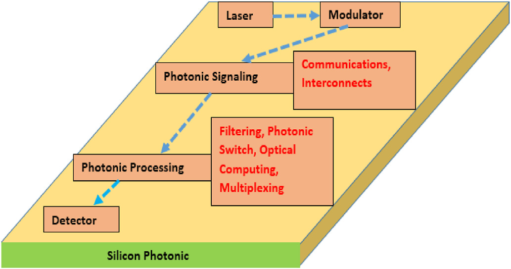
The maturation of silicon photonics technology has raised expectations for its impact in creating vital new applications. These include ultrafast optical communications, distance sensing in self-driving cars, photonic-enhanced computing, and quantum information processing. The unique combination of performance, high yield, and the ability to handle large volumes, facilitated by standardized manufacturing technologies, has contributed to the success of silicon photonics. Currently, thanks to standardized technology platforms in silicon photonics, foundries can access optimized components like low-loss optical paths, rapid modulators, adjustable tuning, swift germanium photodiodes, and highly efficient optical and electrical interfaces. A silicon chip combining microelectronic and photonic circuits could provide unprecedented functions in high-speed computing, communications, and sensing. Such an on-chip integration of microelectronics and photonics technologies could pave the way for significant breakthroughs in realizing high-speed, low-power consumption-based advanced optoelectronic technology. Data centers, for example, would have high-performance computer processors and communications links that are low power, scalable, and consume low power when a large number of microelectronic and photonic circuits are integrated on a single chip. Fig. 1 shows a schematic illustration of the integration of various components on a silicon chip for next-generation optoelectronic technology applications.

Fig1
Achieving the goal of integrating these two technologies on a single silicon chip is quite challenging. Photonic circuits typically employ silicon-on-insulator as a substrate, as opposed to bulk silicon for electronic circuits . Computer processors, memory chips, communication chips, and image sensors are manufactured using complementary metal oxide semiconductor (CMOS) technology. This technology can produce a large number of transistors and electronic circuits onto a single chip, as it is based on silicon. Wafers made of silicon-on-insulator or bulk silicon substrates can be used for this technique . Bulk silicon substitutes are the more popular choice due to their abundant supply chain and low cost . On the other hand, thick wafers are employed in the fabrication process of silicon photonics. There are, however, limitations with thick wafers due to the limited supply chain, and they are also too expensive for many uses, such as computer memory.
Scientists have revealed the most current developments in microelectronics and photonics along with their applications as these fields continue to develop. They are now looking forward for opportunities to merge photonic and microelectronic circuits on a single silicon chip for a variety of industrial applications such as on-chip light source with high intensity and optical switches for high bandwidth communication in data centers. Modern optical chips can be enhanced with electronic functionality by integrating transistors and circuits onto a silicon photonics platform without altering the usual fabrication method used by photonic foundries. This strategy maintains optical excellence and foundry interoperability while including on-chip electrical building blocks to enable optical capability at no additional expense. In a recent development, a transconductance amplifier and an analogue multiplexer for sequential readout of 16 photodetectors, spread in a large-scale design of MZIs, have been integrated to demonstrate the advantages of monolithic electronics. In order to integrate photonic integrated circuits into well-designed optoelectronic systems, their packaging is essential and critical. Since photonic packaging is expensive and limited in throughput, it often poses a significant barrier to scalable deployment of PIC technologies. Additionally, this field is quite recent and will soon revolutionize the global electronic industries [Fig. 2].

Fig2
Recent development of emerging microelectronic and photonic circuits
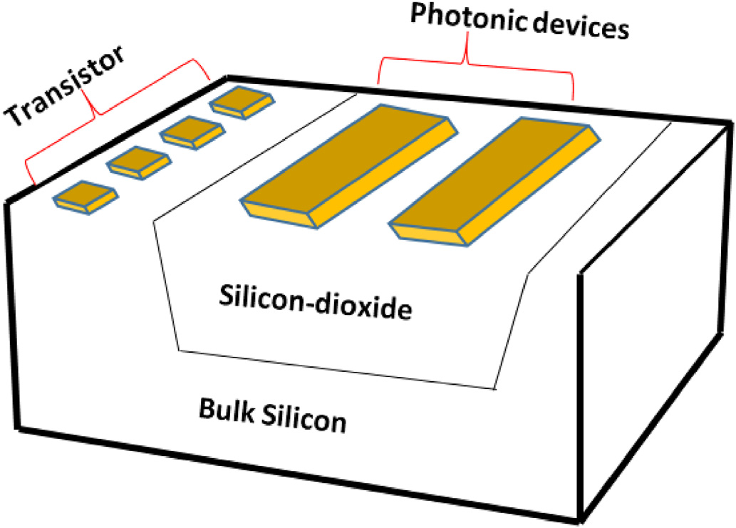
Few strategies have been developed to address the restrictions associated with integrating photonic devices and advanced electronics. Their methodology demonstrates considerable potential for achieving high-speed, energy-efficient optoelectronic technology. The researchers announced the initial achievement of producing photonic devices on a large silicon base. The device was constructed using a vast number of electronic components called transistors (Fig. 3) . This groundbreaking research facilitates the large-scale manufacturing of optoelectronic systems on microchips. Photonics technology was integrated into CMOS chips by depositing polycrystalline silicon over silicon oxide islands (glass). Fig. 3 illustrates the surface of the silicon covered with thin layers of polycrystalline silicon. Afterwards, transistors, which are devices that use photons or electrons, were created from this layer in the silicon-on-insulator area and bulk silicon, respectively.

Fig3
Conclusion
Major technological advances are being made in integrating photonic and microelectronic components and circuits on a single bulk silicon chip. These exciting technological advances are happening at a time when there is an ever-increasing demand for higher-performance optoelectronic technologies that are expected to change the landscape and our daily lives. We are gradually moving from an expensive microelectronic fabrication process to an era of lower-cost processes that yield higher-performing and low-power-consuming technologies. High data rates, deep integration, and optical functionalities have shown silicon photonics to be a formidable foundation for a wide range of communication applications. Despite the above-mentioned advancements, several areas still require work to scale silicon photonic device integration. We list a few obstacles to silicon photonic technologies, such as power loss, which includes the loss due to passive components, delay lines, switches, and chip interconnects, which is a major problem for integrated photonic circuits. The next generation of ultralow-loss components could be made possible via multimode waveguide technology and mixing with silicon or silicon nitride. Additionally, an integrated silicon optical chip is temperature-sensitive; thus, temperature significantly impacts the grating structure used to design optical devices. Therefore, to avoid this influence of temperature, simulation design, and structural design optimization are required. Moreover, these electronic-photonic chips are expected to revolutionize circuit design and enable a wide range of new applications that include high bandwidth, and low power interconnects within chips and highly sensitive biological/chemical sensors and photonic chips for RF signal transmission and processing in cellular networks and radar, just to name a few examples of applications. More technological breakthroughs are anticipated shortly in integrating photonics and microelectronics for various new technological applications. The future of integrated microelectronics and photonics looks bright for systems-on-a-chip evolution.
上一篇: 多孔膜集成到电化学系统中用于生物分析
下一篇: 微机械石英晶体微结构湿法蚀刻