ABSTRACT
Micro-scale electrochemical devices, despite their wide applications and unique potential to achieve ‘More than Moore’s law’, face significant limitations in constructing functional chips due to their inability to integrate with semiconductors. In this study, we propose an electrochemical gating effect and material work function matching criteria, and thus establish the first heterogeneous integration theory for electrochemical devices and semiconductors. Accordingly, we create a novel 3D integration architecture and CMOS-compatible fabrication methodology, including optimizing individual devices, electron/ionic isolation, interconnection, and encapsulation. As a demonstration, we integrate electrochemical micro supercapacitors with a P-N junction diode rectifier bridge circuit and successfully obtain the first monolithic rectifier-filter chip, which shows a revolutionary volume reduction of 98% compared to non-integrateable commercial products. The chip can provide a stable output with a tiny ripple factor of 0.23% in typical conditions, surpassing the requirements of most applications by more than one order of magnitude. More importantly, all the processes are suitable for mass production in standard foundries, allowing ubiquitous applications of electrochemistry in integrated electronics.
INTRODUCTION
Electrochemical devices have been widely investigated as energy storage devices, sensors, displays, and actuators, due to their high-efficiency conversion between chemical energy and electricity. Moreover, integrating micro-scale electrochemical devices with conventional semiconductor chips holds the potential to achieve ‘More than Moore’s Law’ and achieve functionalities hitherto unattainable, such as self-powered chips, implantable health monitoring systems, and fully integrated chemical analytical chips. However, the substantial divergence in intrinsic mechanisms presents a formidable hurdle to achieving a monolithic electrochemical chip, referring to the heterogeneous integration of electrochemical devices with semiconductors on a single chip.
To achieve heterogeneousintegration, it isimperative that the fabrication processes of electrochemical devices and semiconductors are fully compatible, ensuring no interference between the two components and guaranteeing normal chip functionality. However, crucial challenges lie in the distinct fundamental carriers in the fields of electrochemistry and semiconductors: anion/cation for electrochemistry and electron/hole for semiconductors. It results in two systems of different material, process, and operational conditions. For example, the semiconductor process requires high temperatures/pressures to achieve implantation and diffusion, which can damage vulnerable electrochemical materials. Conversely, electrochemical materials tend to disrupt the transportation of electrons/holes, as electroactive ions easily act as extra dopants during long-term service. Therefore, comprehensive design, including isolation and interconnection between devices,material combination, and compatible fabrication, is essential but particularly challenging to achieve heterogeneous integration.
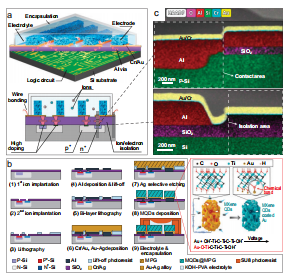
As guided by the above fundamentals, we design the 3D integration architecture of a rectifier-filter chip consisting of electrochemical MSCs and semiconductor diodes, as illustrated in Fig. 2a. The chip can be divided into five parts from Si bottom to top: the semiconductor devices, isolation layer, interconnections, electrochemical electrodes/electrolytes, and encapsulation. Based on the activity difference, we first fabricate a semiconductor P-N junction diode bridge rectifier, which requires high-energy processing at the bottom. The key parameters of the diodes, including junction area, doping concentration, and implantation energy, are numerically simulated and shown in Figs S1 and S2. Above the semiconductor parts, the 350 nm thick SiO2 with contact holes is applied as an isolation layer to provide high electrical/ionic resistance while reducing the field effect brought by the electrochemical gates. Meanwhile, a multi-layer Al-Cr-Au structure is applied as the interconnections according to Equations 1 and 2 and the vacuum energy levels of Table S1. The Al (work function: 4.28 eV) contributes to forming Ohmic contact with deep-doped Si (calculated as 4.62 eV, Note 3), Au (5.10 eV) acts as an inert current collector for the electrochemical devices, and Cr (4.6 eV) serves as the adhesive layer in the middle. Moreover, the Al is fully covered by the Cr/Au to prevent contact with the electrochemical electrode/electrolyte, so that electrochemical side reactions can be avoided.

Fig2
As for the electrochemical MSC part, we first determine the MSC unit should demonstrate a capacitance density higherthan 1.08 mF/cm2 over 120 Hz, according to the filtering signal frequency, load impedance, and desired output ripples (Note 1). Such capacitive performance is hardly achieved by on-chip MSCs. Therefore, we apply two unique strategies to improve the capacitive performance: (1) high-aspect-ratio on-chip framework, and (2) pseudocapacitive quantum dots decoration. The high-aspect-ratio electrode structure provides more electrochemical sites with a limited footprint; pseudocapacitive quantum dots decoration significantly improves the capacitance contribution per electrochemical site, while retaining the ion transport path and makes full use of all accessible electrode area. Those strategies effectively improve the capacitive performance of MSCs yet are more challenging to be implemented under on-chip integration circumstances. Moreover, a seamless encapsulation layer should be applied at the top to isolate the electroactive electrode and electrolyte from the ambient environment.
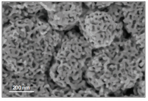
The MSCs, the chip’s core components, are characterized in detail. As shown in SEM images (Fig. 3c–d) of MSC electrodes, the fingers are of 150μmwidth, 30μmgap, and 7μmthickness,separately, bringing a high aspectratio of 0.23 forthe electrode gap. The element maps of the electrode show that the Au and Ti elements are evenly distributed in the vertical direction, which indicatesthe uniform decoration of MQDs on the Au framework. The electrode nanoscale porous morphology is observed with specified SEM shown in Fig. 3e, in which the pore size ranges from tens to hundreds of nanometers, and is abundant for the decoration of MQDs.

Fig3e
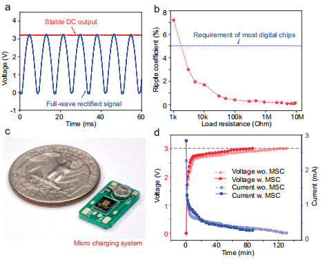
While the filtered output (red) is nearly straight, representing a DC component of 3.2 V and an AC component of 0.0073 V, which brings a tiny ripple factor of 0.23%.Moreover, the ripple factors with varied load resistances are summarized and plotted in Fig. 5b. We can see that the ripple factors decrease with the load resistance and become less than 5% when the resistance is over 3k Ohm. Considering that most digital circuits contain a negative feedback voltage regulation module in the first stage, which brings a vast input resistance over 100k Ohm, it is believed the MSC-based rectifier-filter chip is applicable when serving as a voltage stabilizing module in miniaturized electronics. The rectification-filtering performance is further demonstrated in a micro charging system, which contains a rectifier-filter chip and a micro battery, as pictured in Fig. 5c. The micro charging system can increase the charging efficiency and extend the battery life obviously due to the reduced input signal ripples of the battery. When subjected to a 60 Hz sinusoidal input signal, the micro charging system equipped with a 1 mAh battery can achieve a voltage of 2.8 V in just 22 min (as shown in Fig. 5d). This is a significant reduction of 52% compared to non-filtered charging, which would take 46 min. Moreover, the advantage becomes even more pronounced as the load voltage increases.

Fig5
DISCUSSION
We establish the heterogeneous integration theory for the heterogeneous integration of electrochemical devices with semiconductors, and demonstrate with the first monolithic rectifier-filter chip showing considerable superiorities in performance and size. The heterogenous integration theory, 3D integration architecture and CMOS-compatible fabrication methodology are the keys to the revolutionary performances of the individual devices and monolithic chips. More importantly,the process flowisfull wafer-level, thus providing high throughput and feasibility of mass production in foundries. We believe this work proposes a generalsolution for the integration of various electrochemical devices with modern electronics,whichmay completely change the design rules of integrated circuits.
上一篇: 微机械石英晶体微结构湿法蚀刻
下一篇: 碳化硅独立光子器件的晶圆级集成