1 POROUS SILICON IN PHOTOVOLTAICS
Cost reduction in photovoltaic (PV) solar cells is still an important issue for industry and researchers. In recent years, the cost of PV modules has decreased drastically in Germany. This is, on the one hand, a result of the energy policy of the German government, and, on the other hand, due to the increased PV module production especially in Asia. Most PV modules are made from crystalline silicon (Si) wafers having the advantage of unrestricted resources. Thus, many modern concepts for Si solar cells deal particularly with the cost reduction of the production from which the material costs of Si are crucial.
Usually a Si ingot is cut into wafers by wire sawing. The wafers have a target thickness between 300-700 µm depending on the aspired Si cell process. The sawing process provokes a considerable loss of Si material due to the width of the saw. Therefore, kerfless methods, i.e., methods that require no sawing, are investigated as an alternative process for the production of thin Si solar cells reducing the loss of material. These thin Si solar cells have a thickness below 100 µm. The reduction of the Si cell thickness is further promoted by the fact that the Si wafer accounts for 57% of the Si cell production cost.
Independently from one another, Brendel and Tayanaka have developed the idea of a manifold re-usable Si substrate in the 90ths of the last century. On this basis, the ISFH has established the PSI process, the schematic representation of which is illustrated in Figure 1.

Fig1
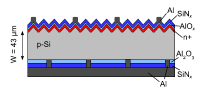
In the first process step of the PSI process, a porous double layer is etched into the Si substrate wafer using a high concentrated hydrofluoric acid (HF) containing electrolyte. The double layer consists of a starting layer with a porosity of about 22% and a thickness of 1.1 µm; underneath there is a separation layer of much higher porosity of about 40% with a thickness of 0.2 µm. The porous double layer serves as the substrate for a subsequent epitaxial step and later on as the predetermined breaking point for the lift-off of the solar cell from the growth Si substrate wafer. The epitaxial step grows a boron-doped monocrystalline Si layer on top of the porous Si layer. The porous layer closes due to the annealing step prior to epitaxy and the pores reorganize. The monocrystalline Si represents the basis for the solar cell, for which existing cell processes are applicable. The epitaxial layer could either be mechanically supported by means of a glass substrate or a metal, however, even processing as a free-standing layer after lift-off has been demonstrated. The schematic structure of a PSI solar cell is demonstrated in Figure 2.

Fig2
The removal of the remaining porous Si from the substrate wafer enables the re-use after lift-off. Steckenreiter et al. demonstrated a 13-fold re-use of the Si substrate, however, a 20-fold re-use is achievable if technical limitations are solved. The most important issue concerning the re-use is the mechanical stability of the substrate, which can be damaged through scratches or occupied by residual porous Si after inhomogeneous lift-off.
2 ETCHING PROCESSES FOR POROUS SILICON
The modification of the Si surface by means of polishing or roughening is essential for the fabrication of solar cells in PV; these are most commonly etching procedures. Etching processes for the formation of porous Si are chemical or stain etching, and electrochemical etching. Before investigating the electrochemical etching in detail, the chemical methods used in PV for the alteration of the Si surface are briefly discussed in the following.
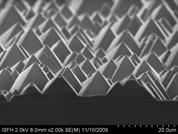
The random pyramid texturization is already a standard process in PV that covers the Si surface with upright or inverted pyramids; an example is demonstrated in Figure 3.

Fig3
For the texturization of crystalline Si hot aqueous solutions based on sodium hydroxide (NaOH) or potassium hydroxide (KOH) are used commercially. Furthermore, K2CO3 solutions are used for the formation of randomly distributed pyramids with an average height of 1 - 2 µm. However, the texturization of multi-crystalline Si surfaces requires acidic solutions since anisotropic etching is not possible due to the lack of a dominant crystal orientation. Here, hydrofluoric acid (HF) solutions with nitric acid (HNO3) are used in mixtures varying from 1:90 to 1:10 for HF(50%):HNO3(70%) [26]. Acidic etching is performed at room temperature. Further modification of the performance is possible by adding phosphoric acid (H3PO4) or sulfuric acid (H2SO4).
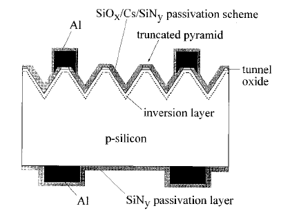
One kind of modification of the pyramidal texturing is reported by Hezel and coworkers. They have invented the truncated pyramids-concept facilitating the formation of small point contacts on the front side of the solar cell; a schematic representation of such a solar cell is demonstrated in Figure 4. The truncated pyramids are performed by a chemo-mechanical polishing step using a slurry of SiO2-particles that follows the conventional anisotropic texturization in KOH solutions.

Fig4
The electrochemical etching process for the formation of porous Si requires holes for the Si dissolution as well. An electric field, i.e., a current that is applied to the Si wafer, forces the holes to move to the Si/HF interface where they react with the fluoride ions. The holes are either present in the bulk Si in case of p-type doping or they are generated through illumination in n-type doped wafers. The following chapter introduces the electrochemical etching processes used in this work in detail.
The formation of porous Si by electrochemical etching was discovered by Uhlir and Turner in the 1950s. Independently they found that a thick porous surface layer forms if Si is electrochemically dissolved below a critical current density. Since then, the characteristics of porous Si as well as the required etching parameters have been investigated by many research groups. Today, porous Si finds widespread application, e.g., as a sensor material or in medicine application. Besides, it is under investigation as an explosive for airbag igniters or as an ingredient of chewing gum. Additionally, porous Si is a promising material in photovoltaics as well.
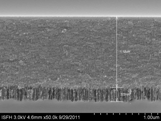
The PSI process as performed at ISFH was introduced in chapter 1.1 on page 2. It requires a mesoporous double layer that consists of a starting layer with a thickness of 1.1 µm and a porosity of about 22% and a separation layer with a thickness of 0.2 µm and a porosity of about 40%. The starting layer is used as a substrate layer for a subsequent epitaxial growth of crystalline Si on top. The separation layer is required for the lift-off of the stack of porous Si and epitaxial Si and serves as a predetermined breaking point. The appearance of a mesoporous double layer before and after sintering in hydrogen atmosphere is illustrated in Figure 5.

Fig5
The images were taken at ISFH by scanning electron microscopy (SEM) with a Hitachi S- 4800. The unsintered porous Si shows pore diameters of about 2 nm and, therefore, it is referred to as mesoporous. For mesoporous Si that was etched with similar parameters a surface area of about 230 m 2 /cm3 was reported by Herino et al. They investigated nitrogen adsorption isotherms using the Brunauer-Emmett-Teller (BET) model.
上一篇: 集成电路中金属氧化物半导体的可靠性研究
下一篇: 化合物半导体的选择性蚀刻