The term etching is used to describe any technique by which material can be uniformly removed from a wafer, or locally removed as in the transfer of patterns during fabrication of a microcircuit. The basic mechanism of wet chemical etches of semiconductors is the formation of an oxide, or oxides on the surface, and the subsequent dissolution of the oxidized products by either acids or bases. Wet chemical etching of any material can be thought of as a sequence of five steps:
1) Transport of the reactant to the surface 2) Adsorption of the reactant 3) Reaction at the surface 4) Desorption of reaction products 5) Removal of reaction products away from the surface
Many etchants have been reported for GaAs, however, very few of them are isotropic. This is because the surface activity of the Ga and As faces is quite different. The As face, terminated on arsenic, has two unsatisfied bonds per atom. Consequently, although some reconstruction occurs in the surface layer, it is still more reactive than the Ga face, and thus etches at a faster rate. As a result, most etches give a polished surface on the As face. The Ga face etches much slower, because it has no unsatisfied bonds, and tends to show up surface features and crystallographic defects. Almost any combination of oxidizer and oxide-dissolver will operate as an etchant. In most GaAs etchants the oxidizer is H2O2. The acid is generally one of the more common ones, such as H3PO4, HNO3, H2SO4, HCl, or C6H8O7. Ammonium hydroxide-hydrogen peroxide mixtures are also popular because of the controlled etch rate of ~3000Å/min for a 1ml NH4OH:700ml H2O2 solution. There are also mixtures that exhibit strong anisotropy.
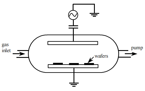
Electrons also drift at a much higher velocity than ions. As electrons gain kinetic energy from the electric field, their effective temperatures increase above the gas temperature. While the temperature of the atoms and molecules in the gas remains near ambient, electrons can attain high average energies, typically 1-10 eV, corresponding to an effective electron temperature of 104 -105 K .(49-51) This energy is transferred to the gas by collision processes in which ions and highly reactive species are created. It is this property of the plasma that allows high-temperature type reactions to occur at low ambient temperatures and permits the use of temperature sensitive materials such as organic resist masks for etching.
The large difference between electron and ion mobilities also creates a sheath near the powered electrode. Since the coupling capacitor suppresses dc current components, electrons can accumulate at the electrode surface which assumes a negative dc voltage superimposed on the time-average AC potential. The powered electrode reaches a "selfbias" negative voltage, VDC, with respect to ground. Similarly, when an electrically isolated surface (such as an insulating substrate isolated from ground by an insulating film) is in contact with the plasma, it must receive equal electron and ion fluxes at steadystate. Following the same reasoning as above, the isolated surface must acquire a negative potential with respect to the plasma to retard the motion of electrons and enhance the motion of ions to equalize the fluxes of both carrier types. The potential of the isolated surface with respect to ground is referred to as its floating potential, VF. As in the case of the grounded walls and the powered electrode, the isolated surface is surrounded by a sheath of reduced electron concentration. The sheaths are typically a few millimeters thick.

Fig1
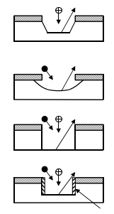
Etch processes are judged by their rate, selectivity, uniformity, directionality, surface quality, and reproducibility. While typical wet etch techniques exhibit excellent selectivity and allow processing in large batches, they suffer from the inability to transfer pattern sizes smaller than about 1µm with the degree of fidelity and control required for the manufacture of VLSI/ULSI devices. Because wet etching is isotropic, the horizontal pattern dimensions must be much larger than the thickness of the film to be etched due to the inherent undercutting. These problems are solved by replacing isotropic wet chemical etching with dry etching techniques. Other advantages of dry over wet etching are the reduced chemical hazard and waste treatment problems, and the ease of process automation and tool clustering.Since most dry etch processes use a low pressure gas in the form of a plasma to provide etchants, dry etching has become synonymous with plasma etching. There are, however, non-plasma etch techniques (such as photo-chemical and vapor etching) that are receiving increased attention and fall in the category of dry etching. While a wide variety of phenomena may play a role, etching mechanisms can be grouped into four basic categories, as shown in Figure 3.

Fig3
The samples used in this study included GaAs substrates grown by liquid encapsulated Czochralski (LEC) which were undoped, semi-insulating (100) orientation and undoped, 5000Å thick Al0.22Ga0.78As layers grown using triethylgallium (TEG), arsine (AsH3), and dimethylamine alane (DMAA) in a Metal Organic Molecular Beam Epitaxy system.
Most of the etching was performed at room temperature (21°C), but temperaturecontrolled baths were used for activation energy determination over the range of 0-90°C. All etching experiments used a two part etch mixture. First, anhydrous citric acid crystals were dissolved in deionized water (DI H2O) at the ratio of 1g C6H8O7:1ml DI H2O. The reaction is endothermic and hinders quick dissolution, so the citric acid is mixed with deionized water at least one day in advance to ensure complete dissolution and room temperature stability. Approximately fifteen minutes before conducting any material etching, the liquid citric acid/water mixture (considered as one part C6H8O7 in this thesis) was mixed with 30% hydrogen peroxide at a given volume ratio (x parts C6H8O7 to 1 part H2O2 by volume). The fifteen minute delay is used to allow the etchant to return to room temperature, if any temperature changes occur due to mixing.
上一篇: HF 基多孔硅电化学蚀刻溶液研究
下一篇: 晶体硅的蚀刻