ABSTRACT
SAC305 (96.5 wt% Sn, 3 wt% Ag, 0.5 wt%Cu) solder is increasingly becoming popular due to its reliability good characteristics and performance in addition to the environmental concerns and regulations that restrict the use of lead in nano/microelectronic products. In nano/microelectronics, manufacturing smooth solder coatings free of defects such as voids and cracks, which can compromise joint reliability is crucial. Magnetron sputering ofers a high degree of control over flm thickness and composition, resulting in flms with excellent uniformity and adhesion. Despite these advantages, fabricating continuous and robust SAC305 flms using magnetron sputering remains a difcult task with limited research addressing these Challenges. To address these challenges and obtain an enhanced surface morphology property, we focus on fabricating SAC305 thin flms by optimizing the magnetron sputering parameters including sputering power and pressure, and by using various substrates. Field emission-scanning electron microscopy imaging, energy-dispersive X-ray spectroscopy, X-ray diffraction, and atomic force microscopy were used to evaluate the quality of the thin flms.
These components are interconnected using solders at various levels to ensure mechanical and electrical continuity. The interconnection technology has advanced from conventional automated wire and tape bonding to fip-chip technology due to reliability, high electrical performance, and package miniaturization. Sn–Pb solder alloys have been widely used in nano/microelectronics due to their low melting temperature and good wetting properties, but they are being phased out due to regulations and Pb toxicity concerns. SAC305 (96.5%Sn–3%Ag–0.5%Cu) solder is evolving as a promising alternative material to Sn–Pb solders due to its low eutectic temperature, exceptional conformity with other components, non-toxicity, and superb mechanical/structural properties.
The rapid evolution of digital electronics, exemplifed by Artifcial Intelligence (AI) and high-performance computing (HPC), has created unprecedented demands for computers with remarkable memory, speed, and computational capabilities. In response to these demands, the number of transistors per unit area on microchips has been exponentially increasing, in line with Moore’s Law, while chip sizes continue to shrink. However, to address the growing complexity of system integration requirements, such as high I/O connections, there is a critical need for the development of smooth and continuous thin flm solders. Such solders must facilitate fast signal transfer, minimize power consumption, and efciently dissipate heat. Achieving a smooth and continuous surface topography in the deposited solder is essential for its efective use in nano/microelectronics applications. Additionally, the microstructure and properties of the solder joints signifcantly infuence their performance. Specifcally, thin flm solders with smooth surfaces and without imperfections yield superior electrical and thermal conductivity, strong adhesion, and exceptional reliability. The microstructural characteristics of these micro and nanoscale solders are not fully understood. Further research could lead to the optimization of the joining processes and improve the electrical properties and reliability of the joints through the establishment of correlations between fabrication, microstructure, and properties.
2 Experimental setup
This study investigated the deposition of SAC305 thin flms on various substrates: silicon (Si), gallium arsenide (GaAs), sapphire (Al2O3), and silicon dioxide (SiO2). A single high-purity (99.99%) SAC305 (96.5 wt% Sn, 3.0 wt% Ag, 0.5 wt% Cu) 2″ diameter and 0.25″ thick target was acquired from ACI Alloys for all flms’ depositions. Before deposition, 100 mm diameter substrates of Si, GaAs, Al2O3, and SiO2 were obtained from University Wafers. The Si and GaAs wafers had a thickness of 500 μm and a (100) crystallographic orientation. The Al2O3 substrate has a thickness of 650 μm, while the SiO2 substrate has the same thickness (500 μm) as the Si and GaAs wafers. All substrates were then sectioned into a 2 × 2 cm squares for the deposition process.
3 Results and discussion
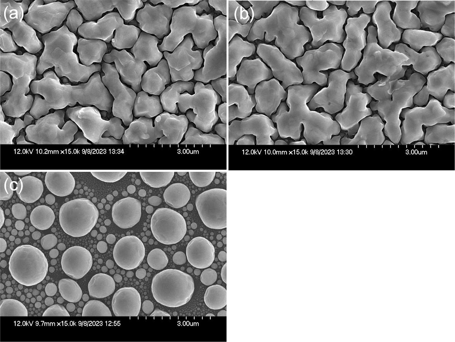
The process parameters were set at a power of 200 W and a pressure of 0.533 Pa. The deposition was conducted at room temperature. The resulting flms exhibited a grain size of 1.65 µm (Fig. 1a). The grain size was determined from the FE-SEM images, and the measurements were analyzed using ImageJ software. However, the flm’s high roughness posed challenges to obtaining surface measurement due to the AFM tip resolution limitations. The flm’s structure was notably porous, marked by the distinct grain boundaries, which made nanoindentation tests practically impossible. The substrate temperature was varied to enhance the flm’s surface morphology; the temperature was increased to 50, and 100 °C while keeping other sputering parameters constant. At 50 °C, the flm’s morphology remained unchanged. At 100 °C, the flm exhibited disconnected spherical grains with signifcant grain boundaries, indicating complete melting (Fig. 1b). During the annealing process, it became evident that the flms that were exposed to lower temperatures for shorter durations remained unafected.

Fig1
Also, the flm’s surface morphology indicated no signifcant changes when the flm was annealed between 120 and 210 °C for 1 to 3 h after deposition. Illustrations of the flms that were annealed between 180 and 210 °C are presented in Fig. 2a–f. However, when the annealing conditions were increased to 220 °C for an hour, the flms underwent noticeable transformations (Fig. 2g). This transformation included grain growth, the development of voids, and, in some instances, disintegration into separated islands on the substrate. The fabricated SAC305 flms’ quality was not improved as a result of the above microstructural transformation. These observations were consistent with the fndings presented by Abbas et al. (2019). Based on these results, the emphasis of the study was shifted to the non-annealed flms, to explore the infuence of varied sputering parameters on enhancing the surface morphology of the thin flms.
In general, DC power is an economical and efective choice for sputering conductive materials such as metals and transparent conductive oxides. Magnetron DC power sputering is easy to control because the amount of current and the thickness of the flms are almost directly proportional besides the resulting sputered flms exhibit high uniformity. On the contrary, RF magnetron sputering power is versatile, making it suitable for the deposition of conductive, semiconductive, and insulating materials. The RF power source alternates between positive and negative polarities. During the positive half-cycle, electrons fow to the target surface, neutralizing the accumulated positive charge and enabling positive ions to bombard the target in the negative half-cycle of the RF voltage. The deposition rate is higher for DC compared to RF sputering and DC sputering produces high adhesion properties since it requires high energy. SAC305 is a conductive material well-suited for both DC and RF processes.
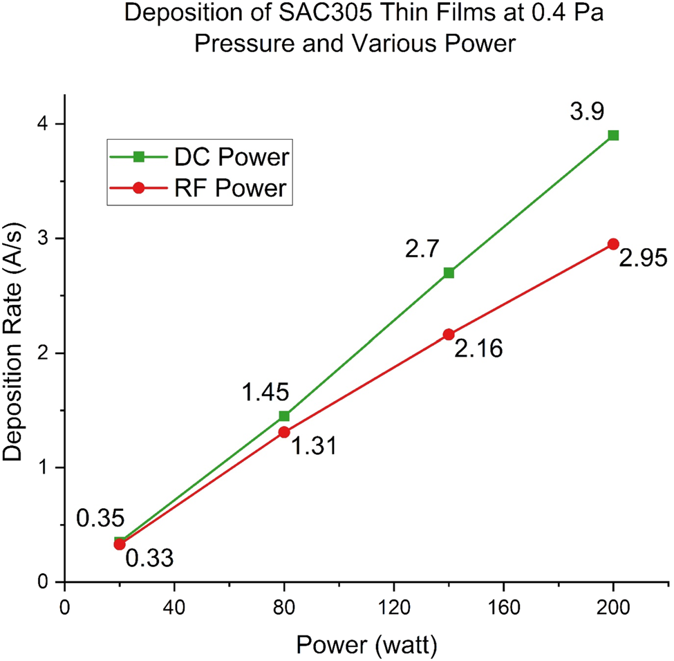
Figure 3 reveals that the deposition rate increases with increased sputering power for both DC and RF sputering processes. This relationship is infuenced by the Ar ion fux and its average energy when it collides with the target. Elevated Ar ion fux at higher power typically leads to pronounced ion interactions with the target. Simultaneously, the enhanced kinetic energy of these ions augments the chances of the incident ions dislodging atoms from the target. Both factors, tied to the applied voltage and sputering power, play pivotal roles in boosting the sputering deposition rate.

Fig3
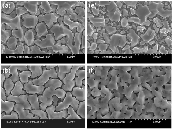
Figure 4 depicts FE-SEM images of the SAC305 flms’ surface area deposited on Si substrate at powers between 20- and 200-wats using DC and RF sources at various pressures. At a deposition power of 20 W, SAC305 flms displayed a fne-grain structure accompanied by larger grain boundaries. The phenomena of smaller grains, combined with voided boundaries, was more profound for RF than DC power. However, when the power was increased to 80 wats, the grain structure for the DC power became denser and the grains were enlarged. A further increase in the DC power supply (140 to 200 wats) did not signifcantly impact the surface morphology. On the contrary, the flms that were fabricated using 20 RF power wats depicted a porous structure and they were not continuous in comparison to the flms that were fabricated using 80 RF. As the RF power was increased (140 to 200 wats), an obvious improvement was visible in the sample surface morphology, accompanied by an increase in grain size.

Fig4
Our focus is still on obtaining continuous robust SAC305 flms and we redirected our atention towards polishing the SAC305 thin flms to enhance the surface morphology. A SAC305 thin flm sputered on a Si substrate was explicitly selected for this polishing treatment. Sample #13 of Table 2 sputered with an RF power source at a pressure of 0.32 Pa and a power of 200W on a Si substrate was unequivocally chosen for this polishing treatment as it depicted the most ideal surface morphology among all the other samples.
4 Conclusion
The results of elevating the substrate temperature beyond 50 °C indicated larger, disconnected, and porous grains, suggesting potential partial melting at 100 °C. It is also noted that annealing efects demonstrated minimal changes up to 210 °C, while signifcant changes, including grain growth and fragmentation, occurred at an annealing temperature of 220 °C for an hour. The lack of observed morphological changes in the annealed samples likely stems from the relatively low annealing temperature (room temperature) compared to the eutectic temperature of SAC 305 (217 °C). Since solidifcation occurs at room temperature with minimal heat release, signifcant temperature-driven modifcations to the surface morphology were not observed for annealing temperatures below the eutectic temperature. We conclude that the optimal morphology of the SAC305 flms was accomplished using an RF power source of 200 W and 0.32 Pa at room temperature. The analysis of the sputering parameters including power and pressure indicated that increased sputering power corresponded to higher deposition rates for both DC and RF techniques, with lower sputering power levels producing porous flms with smaller grain sizes, particularly in SAC305 flms produced using RF sputering power. The deposition rate decreases with increasing the pressure from 0.32 to 2.67 Pa at a sputering power of 200 wats for both DC and RF sputering powers. The use of various substrates for deposition indicated morphological variations and XRD difraction paterns indicated polycrystalline β-Sn grains. The polishing of a selected SAC305 flm on a Si substrate resulted in signifcant improvement in surface roughness.
上一篇: 射频微系统封装工艺技术
下一篇: 微孔膜组件去除超纯水生产中的溶解氧