Abstract
The wet cleaning process at room temperature hasbeen developed for formation of the ultraclean GaN surface. The native/chemical oxide on GaN surface is characterized by XPS. The oxide is suppressed by using this process, and moreover atomic order flatness of the GaN surface is observed by AFM.
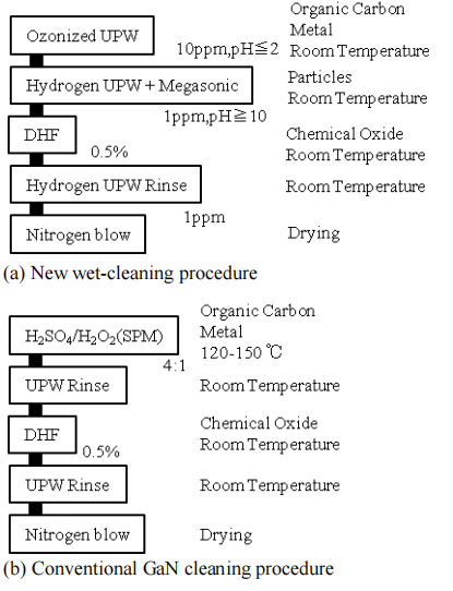
Gallium nitride (GaN) and related materials have been a compound semiconductor commonly used in bright light-emitting diodes, blue lasers, high-power and high-frequency devices with the explosive growth in green technology (e.g., energy saving, smart grids, electric vehicles and renewable power generators) . In order to produce these devices with high-reliability and high-yield, the clean GaN surface is essentially required, and the clean surface is defined as the surface which is free from contaminants such as particles, metals, organic carbons, native/chemical oxides and which features atomic-order surface smoothness. For the achieving the clean surface, the aqueous solution cleaning is often employed, and the cleaning solution is required to be used at room temperature without generating chemical vapor for the process reproducibility and environmental benefits. Our reports have already shown that functional water, for example ozonized water (UPW) and hydrogen UPW, represents a good solution in order to suppress contaminations of metals and particles on the GaN surface. In this study, we develop the new wet-cleaning at room temperature consisting of five-step process. Furthermore, we compare the chemical state of the native/chemical oxide, desorption of organic carbons and atomic-order smoothness of the surface after conventional and new wet-cleanings.

上一篇: 晶圆的湿法蚀刻法和清洁度