Abstract: The literature on polar Gallium Nitride (GaN) surfaces, surface treatments and gate dielectrics relevant to metal oxide semiconductor devices is reviewed. The significance of the GaN growth technique and growth parameters on the properties of GaN epilayers, the ability to modify GaN surface properties using in situ and ex situ processes and progress on the understanding and performance of GaN metal oxide semiconductor (MOS) devices are presented and discussed. Although a reasonably consistent picture is emerging from focused studies on issues covered in each of these topics, future research can achieve a better understanding of the critical oxide-semiconductor interface by probing the connections between these topics. The challenges in analyzing defect concentrations and energies in GaN MOS gate stacks are discussed. Promising gate dielectric deposition techniques such as atomic layer deposition, which is already accepted by the semiconductor industry for silicon CMOS device fabrication, coupled with more advanced physical and electrical characterization methods will likely accelerate the pace of learning required to develop future GaN-based MOS technology.
Gallium nitride (GaN) is a wide bandgap (3.4 eV) semiconducting material with a high breakdown voltage and, as such, is ideal for high frequency, high power and high temperature applications [1]. The use of GaN in commercial electronic devices outside the LED market has until recently been somewhat limited. However, GaN-based high electron mobility transistors (HEMTs) have been commercially available since 2006 and have been used in various wireless applications. The requirement, until relatively recently, that GaN epitaxial layers be grown on a sapphire or SiC substrate has been an economic barrier to more widespread adoption of GaN in many technological applications...
GaN can exist in either a cubic crystal structure (zinc blende phase) or a hexagonal (Wurtzite) crystal structure [24]. The polar hexagonal crystal structure is of most technological interest [25]. Therefore, polar GaN is the relevant surface for this review. The polar surface with Ga face termination is represented by the Miller indices (0001) and the polar surface with N face termination is represented by the Miller indices (000 ). Because GaN has relatively large ionicity, the ionic character of the Ga-N bond and associated electrostatic effects can be expected to play an important role in its structural and electronic properties, which are not as well understood as those of low-ionicity semiconductors such as GaAs [26]. In Wurtzite GaN-based heterostructures grown in the typical (0001) direction, charges trapped in surface and interface states, spontaneous and piezoelectric polarization (the latter in the presence of strain) all contribute to a total charge density at the hetero-interfaces of up to several 1013 cm−2 ...
Most reported investigations into the effect of surface treatments on GaN have been carried out during the fabrication of metal-GaN Schottky contacts, where an important aim is to remove surface contaminants such as oxygen and carbon. Many of the results summarized here are from published reports of such studies. The surface chemistry, the electronic structure of the GaN surface and its atomic structure are important and interrelated factors when reviewing a cleaning process. For metal-polar Ga face GaN interfaces, the performance of the contact depends sensitively on the starting GaN surface. This surface has usually being exposed to atmosphere, thus a native oxide forms which can lead to contact problems in these structures [69,70]. Edwards et al. [71] report the existence of an overlayer on the GaN surface of 2–5 nm thickness, half of which consists of organic and inorganic contamination. The residual material in this layer is assumed to be native oxide. Oxygen at the GaN surface generally bonds to the Ga, consistent with large electronegativity difference for these two elements.
This section will focus on research reported on metal oxide/GaN semiconductor devices. Unless otherwise specified, ‘GaN’ will be taken as Wurtzite-structure n-type (0001) GaN.

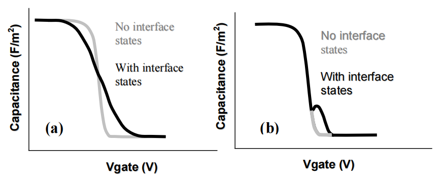
Capacitance voltage measurements are very well understood for the Si-SiO2 system [84]. They can provide a significant amount of information about defects in MOS gate stacks using capacitors (MOSCAPs) rather than transistors, avoiding possible processing-induced artifacts inherent in the more complex fabrication processes required for FETs, and significantly reducing device turn-around time. When applied to semiconductors such as GaN, however, there are a number of factors which should be considered.
上一篇: 氮化镓表面常温湿法清洗工艺
下一篇: 光刻胶的选择标准