INTRODUCTION
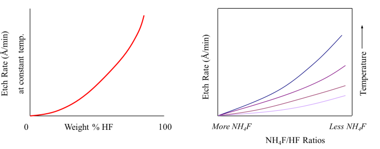
Buffered oxide etch (BOE) is used to remove SiO2. BOE is a very selective etchant, meaning that it stops at Silicon and does not etch further. This etch may be used in a number of steps. BOE can be used at the beginning of the process to define holes in the thermally grown oxide to fabricate contacts with the Silicon substrate. BOE can also be used to define contact (via) by etching the Spin on glass layer. The BOE etch process is based on the following reaction: SiO2 + 6HF → H2SiF6 + 2H2O where H2SiF6 is soluble in water. A buffering agent, ammonium fluoride (NH4F) is also added to the solution to maintain HF concentration and to control pH (to minimize photoresist attack): Buffering reaction: NH4F ↔ NH3 + HF The actual etch rate of the oxide is dependent on a range of factors. For example, deposited SiO2 is etched at a much higher rate than thermally grown oxide.The concentration of HF and NH4F in the solution coupled with temperature also effects the etch rate as seen in the following figures.

Etch rate of SiO2 increases with increasing weight % of HF in the etch solution, as well as higher ratios of NH4F buffer in the solutions. Etch rate also increases with increasing temperature. This process uses highly toxic acids hence it is advised that the following process should be carried out with extreme caution. Careful study of the Material Safety Data Sheet is prescribed before undertaking BOE process. The following document describes in detail the procedure for Buffered Oxide Etch (BOE) of silicon dioxide on silicon wafers.