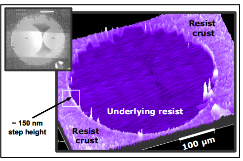
A combination of wet chemistry and high-velocity solid CO2 aerosol pre-treatment was used to remove ion-implanted resist from patterned Si structures. The top resist surface is modified by heavy ion-implantation (1x10¹⁶ As atoms/cm2 , 40keV) forming a crust ~100nm thick. The aerosol treatment, which is aimed at breaking and partially removing the crusted top layer of implanted resist, produces circular openings in this surface, with diameters on the order of tens to hundreds of micrometers. No resist is detected by either optical microscopy or localized SEM inspection, after immersion in hot H2SO4/H2O2 mixture (SPM), on aerosol-pretreated wafer fragments. In contrast, resist residue is still observed on similarly pre-treated specimens, after immersion in either Nmethyl pyrrolidone or Microstrip2001™, even under ultrasonic agitation. Overall, the aerosol pre-treatment is a key step in reducing the amount of resist residue, for both aqueous-based and solventbased wet cleaning. Full-wafer defect-count results, post aerosol treatment, are reported for poly-Si line widths down to 40 nm.
Introduction
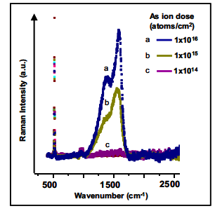
One of the most critical challenges for future generation devices is the effective removal of post-ion-implant photoresist, without damage to underlying gate stack structures (1). Additional requirements for a viable resist strip process must include complete removal of any resist residues, no silicon substrate or dopant loss, and compatibility with novel metal-gate and high-permittivity (high-k) materials. Resist is typically employed as block mask during ion-implantation for front-end-of-line (FEOL) CMOS device processing flows. Since elevated ion doses and energies are necessary for increased device performance, the top resist surface undergoes chemical modification under the ion flux, resulting in the formation of a “crust” which is very difficult to remove at the required high selectivity specifications, by either wet or dry methods. For example, photoresist stripping with aggressive, fluorine-based plasma chemistries leads to unacceptably high silicon substrate and dopant loss. At the same time, wet-chemistry treatments alone can not effectively attack or penetrate the top crust, thus being unsuccessful in removing heavily ion-implanted resist layers. Alternative resist strip methods have been proposed, such as a combination of physical force pre-treatments followed by more traditional wet cleaning steps. For example, the removal of blanket,ion-implanted deep-ultraviolet (DUV) resist (As, 1x10¹⁶ atoms/cm2 , 80keV) from bare Si wafers, using a combination of cryogenic CO2 and wet cleaning techniques has been reported (2). In addition, other previous studies have also reported removal of ionimplanted resist at various doses and energies, using different methodologies such as supercritical CO2 combined with chemical additive formulations (3), a piranha-based process reaching 200°C on-wafer (4), a single-wafer process using sulfuric-acid-based mixtures (5) and an all-dry process consisting of a plasma strip step followed by a pulsating CO2 cryogenic aerosol treatment (6). This paper reports on ion-implanted resist removal studies using a combination of high-velocity solid CO2 aerosol pre-treatment and wet chemistry. Resist specimens are characterized post wet and aerosol treatments using Optical Microscopy, SEM, HighResolution Profilometry (HRP) and X-ray Photoelectron Spectroscopy (XPS). The effectiveness of SPM vs. solvent-based chemistries for implanted resist removal with and without physical force is also evaluated.
Experimental
Both 200mm and 300mm wafers were used for these experiments. The 200mm Si wafers were coated with KrF DUV resist (JSR) in a checkerboard pattern. This allowed for the presence on the same wafer of three distinct surface regions: (i) blanket resist on top of patterned poly-Si, (ii) patterned resist on top of patterned poly-Si and (iii) exposed patterned poly-Si (i.e. no resist present). All resist-coated wafers were subsequently ionimplanted with a dose of 1x10¹⁶ As atoms/cm2 , at 40keV. The post-implant resist thickness was ~350nm. The most aggressively scaled poly-Si lines on the 200 mm wafers were nominally 70 nm wide and 100 nm tall. The 300mm patterned Si wafers, which were used for defect-count studies in the absence of resist, had poly-Si lines with a wide range of width and pitch values, down to 40nm wide and 100nm tall. Wafers were prepared at IMEC and were subsequently sent to the BOC Eco-Snow location, where the high-velocity solid aerosol pre-treatments were performed. The wafers were then sent back to IMEC, where all characterization and wet strip experiments post-aerosoltreatment were performed on wafer fragments, with the exception of full-wafer defectcount inspection, which was done on a 300mm KLA-Tencor 2351 tool.

Figure 1: Raman spectra obtained for DUV (atoms/cm2) resist specimens after ion-implantation with As a 1x10¹⁶ doses from 1x10¹⁴ to 1x10¹⁶ atoms/cm2 at 40 b 1x10¹⁵ keV.

Figure 2: HighResist Resolution crust Profilometry (HRP) 3D scan of an implanted resist layer opening formed by solid aerosol treatment. The insert shows a topdown optical image of Underlying resist the same area.
上一篇: BOE湿蚀刻的硅二氧化
下一篇: 湿法化学处理对锗晶片表面影响的研究