Introduction
Due to its excellent low field mobility [1], germanium has recently re-emerged as an alternative to silicon for high performance devices. As for silicon, appropriate wet chemical treatment of the germanium wafer surface is of the utmost importance for final device yield and reliability. Wet chemical processes need to be developed for germanium cleaning and for surface preparation for subsequent growth processes, e.g. epitaxial growth (an oxide free germanium surface) or for Atomic Layer Deposition (a hydroxyl terminated germanium surface), … In this work, the chemical change of the germanium wafer surface under influence of various wet chemistries is investigated. Surface preparation methods are proposed for both epitaxial growth and for Atomic Layer Deposition (ALD) on germanium.
Experimental
Cz grown p-type <100> germanium wafer pieces were dipped in various chemicals (NH4OH, HF,HCl, HBr, H2O2, …) and subsequently N2-blow dried. Dip time was always 5 minutes unless other wise specified. The samples were stored in a N2-ambient until further analysis. XPS spectra were recorded using a SSX100 equipped with an AlKα anode. The peaks were mixed Lorentzian-Gaussian fitted with a linear or Shirley background. Oxide thickness values were obtained using the Thickogram method [2], which is based on the Hill-equation [3].For etch rate measurements a Scaltec SBC31 balance was used. Etch rates were calculated using ER = 2∆m ρπd 2 ∆t , or by fitting the weight loss vs. dip time curve.
Silicon and germanium are both group IV elements with comparable physical properties although distinct differences exist. Table I summarizes the most relevant ones. Both silicon and germanium form native oxides, which show catenation, but the absence of germanium analogues of silicone polymers speaks for the lower stability of the Ge-O-Ge linkage [4]. In addition, the hexagonal form of GeO2 is water soluble (5.2 g/l) [5]. Furthermore, there is a trend towards increasing stability of MII rather than MIV compounds in the sequence Si, Ge, Sn, Pb [4].


Etching and oxidizing of the germanium wafer
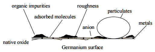
As for any surface, a number of unwanted deposits might be present, as shown in Figure 1. Organic contamination is commonly removed using oxidative chemistries. Particles and metals are generally removed using a combination of oxidation and etching possibly complemented by chelating agents, surfactants and physical action, like megasonic irradiation. In the following paragraphs we will have a look at the effect of frequently used silicon cleaning chemistries on the germanium wafer surface.
下一篇: 用湿化学蚀刻技术制造半导体