INTRODUCTION
Semiconductors such as InGaP and InGaAsSb are important for lightemitting devices as well as communications devices and electronics. Fabrication of these devices is achieved by plasma etching in which an ionized gas mixture etches the substrate by both chemical reaction and physical bombardment. In plasma etching for these purposes, indium products are not as volatile and are usually more di# cult to remove than other semiconductor materials. For this experiment, only wafers with an existing.
epitaxial GaAs cap layer grown over an underlying InGaP layer were available. For the development of an Inductively Coupled Plasma (ICP) etch process for the InGaP layer, the top GaAs layer must "rst be etched o$ to expose the underlying InGaP layer. A common technique used to do this isnvolves a selective wet chemical etch that will remove the GaAs layer without etching or damaging the InGaP layer.1 Determining the selectivity and etch rate for removing the GaAs layer are the primary goals of chemical wet etch development. Once this has been accomplished, a “recipe” for removing the epitaxial GaAs layer can be created. Chemical wet etching selectively removes the cap layer of the wafer through a series of chemical reactions in a liquid solution. For this etch process, H2SO4:H2O2:deionized water, a common solution for removing GaAs, was used in the proportions of 1:8:640. ! e reaction occurs in a sequence of steps involving an oxidation reaction of the hydroxide ions when the semiconductor is immersed in an electrolyte system to produce Ga2O3 and As2O3. !ese oxides dissolve in the acid of the etchant solution and form soluble salts.2 Wafer samples with a 750Å cap layer of GaAs on top, middle layer of InGaP and thick base layer of GaAs were used. !e layer structure of these wafers is shown below. Later etching will use InGaAsSb wafers. However, because indium is the most di# cult layer to etch, InGaP is a good starting point.
RESULTS AND DISCUSSION
Results were inconclusive after the "rst round of the etch process. It appeared that the wet etch solution did not selectively etch the wafers. It was hypothesized that the wafers could have been upside down, meaning that the thicker, bottom layer of GaAs was being etched instead of the 750Å top layer. In the second round of the etch process, care was taken to mark the bottom sides of each sample using a scribe. A control wafer was also used in the second round, which was purposefully %ipped bottom side up for etching. In the second round, a sample from each wafer type was also used. Because the etch solution attacked the photoresist, which can be seen in the negative etch rates in Fig. 3 and in etch depths greater than 750Å in Fig. 4, the wafers had to be stripped of the PR to measure accurate etch depths. ! is was done by agitating the wafers in acetone for 2 minutes, rinsing with methanol for 2 minutes, and blow dry-ing the wafers with nitrogen. !e process was repeated until all of the photoresist was removed. !e wafers were then measured again with the pro- " lometer to determine the actual etch rate and depth. Reproducible etch rates were achieved as shown in Fig. 3. !e etch rate for samples stripped of PR averaged 8.37Å/s with a standard deviation of 0.92Å/s, which was near the expected etch rate of 10Å/s.

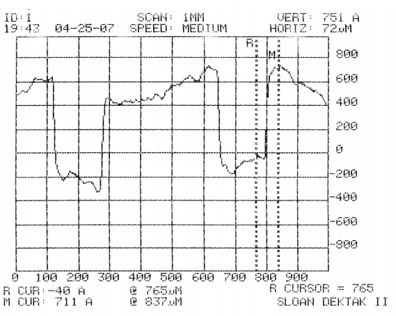
Fig. 2 is an example of the results from the pro# lometer, which gives a cross-sectional view of the wafer. !is sample was in the etchant for 110 seconds and was stripped of photoresist. !e results show that this particular sample was etched to a depth of 751Å. Because measurements were taken in angstroms (1 x 10⁻¹⁰ m), some experimental error is to be expected using the instruments available. ! ere may also be slight variations in the thickness of the grown layers.