1. Introduction
The manufacture of integrated circuits is a complex and costly process that involves hundreds of steps and requires the monitoring of many process parameters throughout the production process. Today, even using highly automated and precisely positioned equipment located in a near-dustfree clean room and operated by well-trained process engineers, the occurrence of point defects still cannot be avoided (Kuo et al., 1998; Kuo and Kim, 1999). Since clustered point defects on a wafer are often due to process problems or human mistakes, information about cluster size, geometric shape, and spatial location is extremely valuable to process engineers seeking to recognize potential production problems. In general, defect patterns can be regarded as a superposition of two main components acting independently (Friedman et al., 1997; Hansen et al., 1997): the fifirst is random point defects (particle related) and the second is systematic clusters (process related). Random point defects are often regarded as being due to problems in the clean room and tend to rise and fall with the overall cleanliness of the environment. Systematic defects caused by assignable cause are, however, usually attributed to process equipment faults and/or human mistakes.
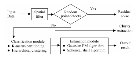
Reducing random point defects needs a long-term gradual improvement in clean room operation protocols or an expensive equipment overhaul, however, removing systematic defects requires a series of automatic detection and classifification processes. An important objective of defect recognition (including defect detection and defect classifification) is the early identifification of process problems (Chou et al., 1997). Defect detection consists in removing the random defects from the measured data (denoising) whilst defect classifification consists in sorting systematic defects into a set of predefifined and meaningful categories. The defect patterns on a wafer contain useful information which can be used to highlight potential manufacturing problems for example: (i) an elliptical zone often arises due to problems in the thin fifilm deposition process; (ii) a circular ring is due to problems in the etching step; and (iii) a linear scratch is a result of machine handling problems (Chen and Liu, 2000; Liu et al., 2002). In addition, if the pattern is located around the wafer center (bulls eye) or along the wafer’s edge (circular ring), this may be a result of nonuniformities created in the thin fifilm deposition process or an uneven temperature distribution during the rapid thermal annealing process (Hansen et al., 1997). Therefore, identifying meaningful defect patterns on a wafer and relating them to their root causes is a critical step towards successful semiconductor manufacture. Traditionally, the problem of defect recognition is addressed through visual inspection by quality engineers usinga scanning electron microscope. This manual approach results in numerous misidentififications and is expensive in terms of personnel costs. Since the large amount of data generated in semiconductor manufacturing makes manual checking extremely time consuming and relatively diffificult, current research (Chou et al., 1997) is focused on delegating this task to Automatic Defect Detection (ADD) and Automatic Defect Classifification (ADC) processes. Automating the detection and classifification processes leads to: (i) a reduction in the operator workload; (ii) more defects being reviewed; and (iii) an improvement in both the accuracy and consistency. The expected reduction in individual chip size coupled with an increase in the size of processed wafers from 8 inches to 12 inches means that techniques such as ADD and ADC are becoming increasingly desirable. In real applications, however, it is quite diffificult to determine the number of systematic clusters and then to separate the convex (linear scratch, elliptic zone) and nonconvex (circular ring) defect patterns simultaneously. Therefore, an integrated approach composed of a spatial fifilter, a classifification module and an estimation module is proposed to solve these problems. The remainder of this paper is organized as follows. Section 2 reviews the relevant literature and model formulations are presented in Section 3. In Section 4, experimental studies are reported. Conclusions are drawn in Section 5.

Fig. 1. Automatic recognition of defect patterns.
上一篇: MEMS 微细加工中的真空辅助湿法加工
下一篇: 薄晶圆处理挑战和新兴解决方案