Temporary bonding attaches substrates to a carrier so that after thinning to the desired thickness further backside fabrications steps can be conducted with “normal” process flows in standard semiconductor equipment. The selection of a suitable temporary adhesive is key to the success of thin wafer handling. The major requirements of temporary adhesives are related to its process flow, thermal stability, chemical resistance, and mechanical strength. The ideal thermal stability should allow high temperature processing up to 400C for dielectric deposition in high aspect ratio vias, polymer curing, solder reflow, metal sintering, permanent bonding or other high temperature processing. The adhesive must be resistant to the chemicals commonly used after wafer thinning. Mechanical strength is required to hold the thin wafer rigidly during processing, especially during permanent bonding applications otherwise the thinned wafer will flex and prevent bonding. The challenge arises in finding a simultaneous solution to these problems while allowing for the gentle release of the thinned substrate to its final, permanent substrate or package without yield loss or stress. This paper will highlight some of the more recent solutions for thin wafer handling that have emerged through technology innovation.
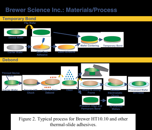
There are three leading candidates for temporary bonding for CMOS and 3D applications†. WaferBOND® HT10.10 made by Brewer Science Inc.[1], T-MAT by Thin Materials AG [2], and the 3M™ Wafer Support System[3] all use polymer materials to support device wafers on carrier for backside processing. Each of these materials has been shown to be successful for thin wafer handling although the details and process flows vary dramatically between each type of material [4]. Brewer Science Inc. WaferBOND® HT10.10 HT10.10 is a thermoplastic polymer adhesive that is spin coated onto the substrates. The higher viscosity of temporary adhesives benefit from advanced coating system such as the SUSS MicroTec SC200/300 coating modules that utilize reverse radial hyperbolic dispense motion and closed covers to achieve extremely uniform coverage. Thickness uniformity of the adhesive is a critical parameter to the thin wafer uniformity. After prebake of the adhesive the surface is not tacky although it is not fully cured. Bonding of the wafer to the carrier can be carried out in a low force thermal compression bonder such as the SUSS MicroTec LF200. Bonding is normally a center-on-center alignment between the carrier and the device wafer. The carrier can be oversized relative to the substrate wafer by a few millimeters to provide edge support. The bond process is done in vacuum at 180-200°C with less than 8KN force.
The primary distinguishing property between the various temporary bonds are the methods of debonding after backside processing. HT10.10, like waxes and high temperature Polyimides, is a thermal plastic material. By definition the material becomes soft as the temperature rises and the substrates can be slid apart. The so called thermalslide approach is easily visualized but requires significant finesse in application. The thinned device wafer is often 25-75µm thick and will crack from shear forces if not properly supported during the thermal slide process. Proper thermal controls are needed to ensure the interface remains at a semi-fluid state with uniform viscosity during the debond.

上一篇: 半导体晶片缺陷模式的检测与分类