A single wafer cleaning system with full coverage back-side megasonics has been developed for pre-lithography backside cleaning processes. Backside particle removal efficiency (PRE) of >95% at ≥65nm for Si3N4 particles was achieved with DIW only, demonstrating enhanced particle removal at both smaller and larger particle sizes with full coverage megasonics. PRE values of >99% were attained by using dilute HF/SC1 chemistry and by increasing megasonics power with SC1. The single wafer clean system allows DIW to be dispensed on the frontside if desired to minimize chemical contact on the device side of the wafer while chemistry is applied to the backside. Etch rate tests confirmed no flow of chemistry to the frontside of the wafer. Field data have shown that full coverage megasonics cleaning can reduce the maintenance frequency of lithography tools. Wafers processed with conventional megasonics or non-megasonics processes encountered subsequent chucking or focusing problems resulting in significant down time of the lithography tool, whereas these issues were not encountered for those wafers cleaned with full coverage megasonics.
As the technology node scales down to 65nm, wafer backside cleaning has become critical due to tight depth of focus and overlay tolerances in critical lithography steps such as shallow trench isolation, gate patterning, and contacts. These steps require that no large particles (0.2µm at 90nm/65nm node) are on the wafer backside. As the technology node scales down to 45nm and beyond, more critical lithography steps will require backside pre-cleaning. In addition, particles and metal contamination on wafer backsides and edges have the potential to contaminate handling surfaces of process and metrology tools. Backside cleaning can eliminate cross-contamination among wafers that come in contact with these tools. For example, some researchers have studied removal of backside Cu to avoid cross-contamination [1, 2].
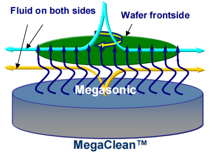
Cleaning experiments discussed in this paper were conducted in Applied Materials SWC chambers which are a part of OASIS CLEAN™ system. This SWC chamber uses a novel, full wafer coverage, 300mm megasonic transducer and dispenses fluid on both sides of the wafer. Acoustic energy is transmitted through the wafer, as shown in Figure 1.

The megasonic frequency was set at 875MHz for all tests. Test Wafers and Metrology High grade 300mm Si wafers (incoming <100particles @≥65nm) were used for preparation of PRE wafers. Wafers were deposited with approximately 10000 Si3N4 particles @≥65nm using a model 2300D particle deposition system (MSP Inc., Minneapolis, MN). Particle measurements were performed using a SP1-TBI wafer surface scanner (KLA-Tencor Inc, San Jose, CA) at ≥65nm with 3 mm edge exclusion. Typical SP1 pre-scan of particle wafer deposited with 0.1µm Si3N4 particles is shown in Figure 2. PRE is defined as (post clean count – pre deposition count) / (pre clean count –pre deposition count) *100. For backside clean PRE evaluation, wafers were flipped upside down using a wafer wand and placed back into wafer cassette. After process wafers were manually flipped back to the upside position with a wafer wand. Thermal oxide 300mm wafers with initial oxide thickness of 500Å were used for etch rate tests. Film thickness was measured at 49 points with 3 mm edge exclusion using a Spectrum FX-100 (KLA-Tencor Inc, San Jose, CA).
上一篇: 薄晶圆处理挑战和新兴解决方案
下一篇: 单晶刀清洗过程:分散现象对冲洗时间的影响