Introduction
All the measurements and methodology presented here are based on CMOS 65nm technology obtained in the state of the art 300mm Crolles 2 plant, Alliance between Freescale, Philips & ST.
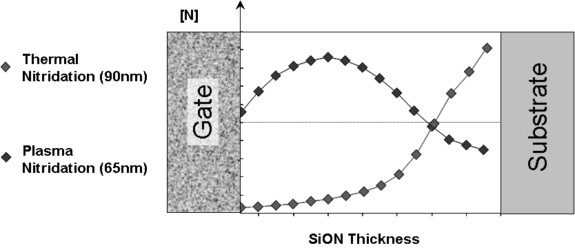
Some devices require Triple Gate Oxides integration, on the same die (fig. 1). The first one is dedicated to Input/Output function. The second one, LP(Low Power) is for low current consumption, and the last one, GP(General Purpose) for high speed applications. Several wet processing steps are used and interact with LP gate oxide. These oxides are produced thanks to Rapid Thermal Oxidation, plasma Nitridation and a PNA(Post Nitridation Anneal) (fig. 2). Three main parameters must be tightly controlled to get reproducible and accurate devices performances: thickness, nitrogen in depth profile and content. Whereas nitrogen lays at the interface oxide-substrate in 90 nm node, it is incorporated closer to the top surface in 65 nm node, to prevent any NBTI issue (fig. 3) [1] [2] These dose profile graphs are obtained by a two steps process: a wet bevel etch followed by XPS measurement along the wafer diameter. Two kind of bevel etch profiles are possible: Top to Bottom in case of a slow dip in a HF bath or radial profile on a spin etcher. This innovative method has been calibrated with conventional SIMS (fig. 4) [3].
