Abstract
Single-wafer die-level fusion bonding (SDFB) process is proposed, which can reduce the mask number and fabrication time in the prototype research of multilayer fusion bonding devices. The conception and scheme are illustrated using micro gas turbine of MIT as an example. The techniques to etch different mask and depth in a single-wafer are listed and analyzed. The alignment compensation mechanism in the SDFB is also discussed which can avoid the photolithography misalignment and improve the precision between key layers. The advantages and disadvantages of SDFB are analyzed in detail. The feasibility of the scheme is verifified by the experiment. Besides micro gas turbine of MIT, the SDFB process can also be used in other multi-layer fusion bonding devices such as ultra thick proof mass inertial sensors, multi-layer flfluidic devices, etc.
1 Introduction
One of the key advantages of MEMS devices is the batch fabrication and the related low cost of the devices, which are usually the main driving force in many applications (Janson et al. 1998; Wolffenbuffel and Mullem 2001). But for some complex devices that need multi-layer bonding process, such as micro gas turbine of MIT, the fabrication time can be very long, which is unnecessary because the advantage of batch fabrication refer to the fifinal productfabrication stage instead of the R&D stage of novel devices. Furthermore, the increase of the fabrication time leads to the reduction of error tolerance for the design and every R&D fabrication steps. A potential way to solve this problem is the single-wafer die-level fusion bonding (SDFB), which can reduce the fabrication time and increase the error tolerance of the design and fabrication processes. Once the device prototype is verifified by the experiment, the batch fabrication and design optimization can be performed more effificiently.The structure of this paper is as follows. The motivation of SDFB is introduced above. In Sect. 2, the conception and scheme of SDFB are introduced and the problem of the different pattern and etching depth in a single-wafer is solved by three methods. In Sect. 3, the advantages and disadvantages of SDFB are analyzed. In Sect. 4, the alignment compensation mechanism between key layers during SDFB is discussed. In Sect. 5, an experiment is performed to verify the feasibility of the SDFB process. Section 6 is the conclusion of the paper.
2 Conception and scheme of SDFB
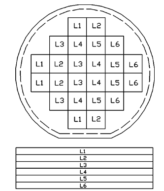
Using six-layer micro gas turbine (i.e., micro-turbocharger) of MIT as an example (Mehra et al. 2000), the conception and scheme of the single-wafer die-level fusion bonding are illustrated in Fig. 1, where ‘‘L’’ represents ‘‘Layer’’. The six layers (layer 1 to layer 6) needed for the turbocharger are fabricated in a single-wafer. In the traditional multi-wafer wafer-level fusion bonding (MWFB) process, there is one DRIE mask on the front and back side, respectively for layer 1 and layer 6, two DRIE masks on one side for layer 3 and layer 4, three DRIE masks on one side and two on the other for layer 2 and layer 5.

Fig. 1 The basic conception and scheme of the SDFB process. The top fifigure shows the single mask scheme for the micro gas turbine and the bottom fifigure shows the bonding scheme after diesaw, the dimension is not drawn in proportion in the fifigures
Three methods are used to fabricate the six layers with different patterns and steps in a single-wafer. One is to adjust the design parameter. In this example, the etching depth of layer 1 and layer 6 can be adjusted to be the same with layer 3 and layer 4 (with the rotor fabricated separately, layer 3 and layer 4 can be fabricated by both sides etching); the other is to use double mask etching and half oxidation shallow etching (Fedder et al. 1996; Dong et al. 2005), which is necessary for fabricating layer 2 and layer 5 together with layer 1, layer 3, layer 4 and layer 6; and the third is hand-painting of some of the dies during the process, which can be used to fifine tune the etching depth of the different layers. The methods mentioned here make it possible to fabricate the structure of these six layers in a single-wafer. After die-saw of the wafer, these six layers can be bonded directly, together with the rotor fabricated separately.
3 Comparison between MWFB and SDFB
For the MWFB, bubble capture, total thickness variation (TTV), wafer bow, surface roughness, surface cleanness and pressure are critical issues (Liu and Devoe 2001; Goh et al. 1994). Bubbles are captured during the bonding process when there’s more than one initial contact point. It may also be caused by the roughness and bow of the bonding wafer. In the MWFB, the fabrication yield has a direct relationship with the bubble problem. For somespecifific pattern, an extra mask may be needed to etch cross-line trenches on the wafer so that the captured bubbles can be connected through these channels to the outside environment. In the SDFB, as the bonding surface area is much smaller than that of the whole wafer, bubbles are more diffificult to generate and usually no extra mask is needed. The fabrication yield is expected to increase correspondingly. Similarly, as the bonding area decreases in the SDFB, TTV is not a critical parameter any more. In the MWFB, the direct bonding wafer number is often limited to avoid contamination, and the unbonding surface should be protected during the process, which requires the remaining of the dielectric fifilm on one side of the wafer and leads to the wafer bow. While in the SDFB, the bonding can be performed directly for all the layers, so the protective dielectric fifilm on both sides of all wafers are stripped before the bonding process, which leads to less residue stress and minimum wafer bow. Surface cleanness is a controversial problem in the SDFB. In one hand, the less mask number and process time mean less contamination, and surface cleanness can be kept better. In the other hand, the diesaw process makes it easier to contaminate the surface with chips and particles generated during the diesaw. In our experiment, we protect the surface by double layer fifilm (one oxidation and one photoresist) before diesaw on both sides of the wafer. The experiment recipes and results will be discussed in Sect. 5. Even not absolutely necessary, high pressure can contribute to a good bonding. The pressure of SDFB can be achieved one or two order higher than that of MWFB due to the bonding area decreasing. Furthermore, the SDFB scheme facilitates the specifific jig design so that the pressure can be maintained during the annealing process.

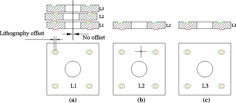
Fig.2Illustrationofalignment compensationofSDFB.aThe cross-sectionoftheassembly structureandtopviewoflayer 1.bThecross-sectionandtop viewoflayer2.cThecross- sectionandtopviewoflayer3.Thebigcirclesinthemiddleof thepiecesrepresentthereal patternofthedevice.‘‘L’’ represents‘‘layer’’
上一篇: 晶片光刻胶处理系统
下一篇: GaN 基金属氧化物半导体器件