Si-based semiconductors-related technologies are well developed for their applications in electronic devices and integrated circuits (ICs). However, the properties of Si-based semiconductors are seldom being applied in high-frequency and high-power systems. In comparison, the GaN-based semiconductors have also aroused huge interests in recent years owing to their advantages, such as wide and direct energy bandgap, better thermal and chemical stability, and high-electron drift velocity. Therefore, GaN-based semiconductors are widely utilized in electronic devices, including field-effect transistors (FETs) (Khan et al., 1993; Zolper et al., 1996; Klein et al., 1999; Yoshida & Suzuki, 1999; Johnson et al., 2000; Zhang et al., 2000; Jiménez et al., 2002; Binari et al., 2002; Braga et al., 2004; Wallis et al., 2005; Horio et al., 2005; Hong & Kim, 2006; Saripalli et al., 2007) and high-electron mobility transistors (HEMTs) (Egawa et al., 2000; Karmalkar & Mishra, 2001; Vetury et al., 2001; Islam et al., 2002; Koley et al., 2003; Khan et al., 2003; Mizutani et al., 2003; Lu et al., 2003; Meneghesso et al., 2004; Fareed et al., 2005; Inoue et al., 2005; Seo et al., 2008). Among the devices mentioned above, GaN-based HEMTs possess high electron mobility larger than 1000cm2/Vs at room temperature and large operating current due to the formation of two dimensional electron gases (2DEGs). In addition, the GaN-based optoelectronic devices, such as light-emitting diodes (LEDs) (Han et al., 1998; Chang et al., 2004; Fujii et al., 2004; Wierer et al., 2004; Shen et al., 2006; Lee et al., 2006; Chang et al., 2006; Lee et al., 2007; Chen et al., 2007; Chuang et al., 2007), photodetectors (PDs) (Kuksenkov et al., 1998; Walker et al., 1998; Katz et al., 2001; Rumyantsev et al., 2001; Sheu et al., 2002; Seo et al., 2002; Pau et al., 2004; Su et al., 2005; Vardi et al., 2006; Navarro et al., 2009), and laser diodes (LDs) (Nakamura et al., 1996; Nakamura et al., 1996; Saitoh et al., 2003; Suski et al., 2004; Schoedl et al., 2005; Peng et al., 2006; Laino et al., 2007; Braun et al., 2008; Rossetti et al., 2008), have also been investigated and developed extensively for display, lighting, memory system, and communication system in recent years.

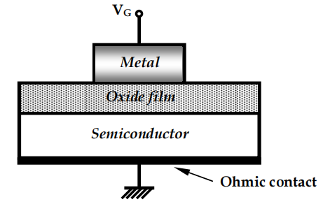
Three typical situations are normally occurred at the semiconductor surface, including accumulation, depletion, and inversion, depending on the applied bias between the two electrodes. Fig. 2 shows the energy band diagrams of an ideal MOS diode with n-type semiconductor at different operating conditions (Neaman, 1997). When a positive voltage is applied on the gate electrode of the MOS diode, the free electrons in conduction band of the semiconductor are driven towards the oxide/semiconductor interface, where electrons are accumulated. Accordingly, the energy band at the semiconductor surface is bent downward and the conduction band edge becomes closer to Fermi level. This is so-called accumulation case, as shown in Fig. 2 (a). When a small negative voltage is applied, the electrons are driven away from the oxide/semiconductor interface by the surface electric field which results in the formation of a depletion region. This case is called depletion case, as shown in Fig. 2 (b). When a larger negative bias is applied, a large number of minority carriers (hole) were induced at oxide/semiconductor interface. Therefore, the energy bands bent upward even more so that the intrinsic level at the surface crosses over the Fermi level.
The number of holes (minority carriers) at the semiconductor surface is larger than the number of electron (majority carriers), and in which case it is called inversion and shown in Fig. 2 (c). However, the situation is different for GaN-based MOS diodes, within which the inversion layer is hard to form because the GaN-based material is a wide energy gap semiconductor. The reported results showed that the generation rate of the minority carriers (holes) is extremely low at room temperature (Casey et al., 1996; Hashizume et al., 2000). For an n-type GaN-based material with a carriers concentration of 1.2×10 17cm–3, the generation time of minority carriers is t 4.2×10¹⁸s. However, it is impossible to form aninversion layer with an extremely long generation time. When a negative bias is applied, there are an insufficient number of minority carriers present at the interface and the depletion region extends into GaN to maintain electric neutrality. Consequently, the n-type GaN-based MOS diodes show a deep depletion characteristic at negative bias.
The GaN-based metal-oxide-semiconductor field-effect transistors (MOS-FETs) is a device which consists of two ohmic electrodes and a MOS diode. Those two ohimc electrodes, located at the two sides of the gate electrode, are connected to GaN-based semiconductor through doped regions. One of the contacts is called the source as it implies that the charge carriers entering the channel originate from this contact, while the other is the drain where the carriers leave the channel. The conductance of the semiconductor near the interface under the gate electrode can be modulated by applying gate bias, as mentioned above for the MOS diode. By applying gate bias, one can modify the effective channel thickness by varying the width of the depletion region, and this in turn varies the output current. If a negative gate voltage is applied on n-channel, the carriers are then depleted from the channel, causing a decrease of the channel conductance; in this case the device behaves as a normally-on (depletion) GaN-based MOS-FETs.
上一篇: 单晶片工具上的栅极氧化物清洁
下一篇: MEMS 器件的金属晶圆键合