Abstract
Metal fifilms can be used as bonding layers at wafer-level in MEMS manufacturing processes for device assembly as well as just for electrical integration of difffferent components. One has to distinguish between two categories of processes: metal thermo-compression bonding on one side, and bonding with formation of an eutectic alloy layer or an intermetallic compound. The difffferent process principles determine also the applications area for each. From electrical interconnections to wafer-level packaging (with special emphasis on vacuum packaging) metal wafer bonding is a very important technology in MEMS manufacturing processes.
Wafer bonding plays an important role in Micro-Electro-Mechanical Systems (MEMS) applications as a technique used for joining substrates. The need to address the large applications variety was the driving force for the development of difffferent wafer bonding processes. Among the wafer bonding processes currently used for industrial applications can be mentioned direct bonding (also known as fusion or molecular bonding - adhesion is generated by chemical bonds between the molecules on the two surfaces) [1], anodic bonding (used to bond a Si wafer to a glass wafer - bond appears due to an oxide layer grown at the interface) [2], adhesive bonding (using intermediate layers, typically polymers) [3, 4], eutectic bonding (bond occurs through an eutectic alloy layer grown at the interface) [5] or intermetallic bonding [6] and thermo-compression bonding (metal bond – bond occurs between two metal surfaces pressed together under heating) [7].
Physical, chemical, electrical, and thermodynamic properties of the given material play a crucial role in the feasibility of the bond process and must be considered already at the design stage of an application. Wafer bonding process selection is based on various criteria related to the materials used (substrates types, bonding temperature and thermal profifile) as well as to the desired application (type of bond – mechanical connection, electrical or thermal conductivity of interface, optical properties and device working temperature).
This paper proposes an overview of wafer boding processes based on metal layers and introduces the process selection criteria for metal bonding.

2.1. Eutectic wafer bonding
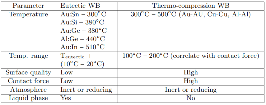
Eutectic alloy is formed at the bonding interface in a process which goes through a liquid phase: for this reason, eutectic bonding is less sensitive to surface flflatness irregularities, scratches, as well as to particles contamination compared to the direct wafer bonding methods. Some of the main eutectic alloys used for wafer bonding applications are listed in Table 1. For a successful eutectic bonding process it is very important that bonder assures a good temperature uniformity across the entire wafer surface and also to control very well the temperature value (avoid overshooting the set point) in order to have a reliable process.
An example of a thermal profifile general shape is presented in Fig. 1. Experimental results showed that good quality bonded interfaces are obtained when temperature is fifirst raised to a value lower than the eutectic temperature, maintained constant to reach uniform heating of both substrates, than increased again to a temperature exceeding the eutectic point with 10–20◦C (depending on specifific process conditions and on substrates restrictions) followed by cooling down to a temperature below the eutectic temperature. Temperature ramp for heating/cooling processes are important and have to be selected based on substrates materials (to avoid thermal shock for dissimilar materials) as well as on device requirements (heating/cooling in vacuum or both or only single wafer in contact with heaters).
上一篇: GaN 基金属氧化物半导体器件
下一篇: 单晶片工具上的栅极氧化物清洁