Pre gate oxide and especially “Double Gate Oxide” cleans are the most critical surface preparation steps in the semiconductor industry. This paper describes the key parameters to perform this kind of operations on a fully integrated single wafer cleaning tool. This switch from conventional batch cleaning tool enables significant defect density reduction and therefore yield enhancement. Nonetheless the main challenge of the double gate oxide clean is the prevention and the control of photo lithography resist lift off during the wet etch. This clean is also composed of two other steps, less critical. Nonetheless special care has been considered in the surface preparation in order to avoid any electrical mobility degradation.
Introduction
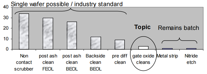
Over the last few years, the number of surface preparation steps in a typical CMOS flow increased drastically with the device complexity. It has been multiplied by five from 0.7µm to 45nm critical line width, representing 40% of a 45nm CMOS process flow. Indeed latest BEOL architecture require higher amount of metal layers and FEOL has higher amount of photo lithography masks for the introduction of system on chips where several options are embedded (DRAM, non volatile memory, analog, RF, …). Moreover, lithography requires cleaner and cleaner surfaces, which has made the scrubbing activity explode. Similar trend has been observed for the post ash cleans with greater need of masks. Only the pre-diffusion cleans amount remains almost unchanged. Recently single wafer cleaning tools are continuously replacing batch tools in the semiconductor industry (figure 1). The driving forces of this revolution are: process flexibility, cycle time, defects reduction and yield improvement. This trend started with BEOL cleans, followed by FEOL applications. Three steps haven’t yet become industry standard on single wafer tools: HF Last before epitaxy or metallization [1], silicide clean, and DGO (Dual gate oxide) cleans which is the topic of this paper.

Figure 1: repartition of surface preparation steps in a 45nm CMOS process flow
Motivation
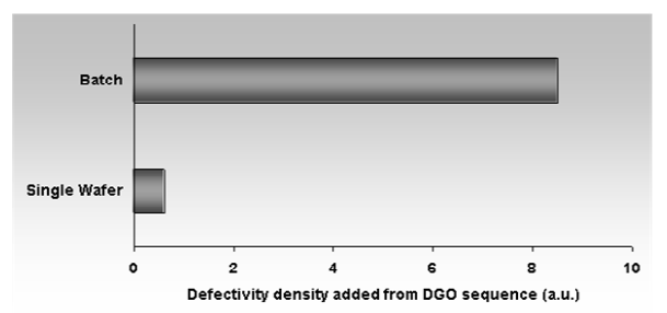
DGO process is the most critical clean in a CMOS flow, directly affecting transistors performance and reliability, which made engineers reluctant to transfer this process from the well established batch systems to single wafer platforms. Nonetheless, the latter present huge advantages by enhancing defectivity (figure 3a) and yield. Metallic contamination is more likely accumulated in batch tools, resulting to severe device performance loss. Whereas single wafer cleaning tools are safer, spray or immersion systems induce films / particles delamination from wafer bevel to deposition on dies (figure 3b) [2]. Contamination is mainly coming from the wafer handling, lot to lot cross contamination or backside to front side particles / films transportation (“Holy Grail” effect [3]). Since few years a lot of efforts have been spent on batch tools to be able to remove such defects without great success, cavitation being difficult to control in immersion tools.

Figure 3a: Defectivity after polysilicium gate deposition in DGO sequence, measured with KLA28000 inspection tool. Single wafer cleaning tool reduces significantly defect density compared with batch tool.
上一篇: MEMS 器件的金属晶圆键合
下一篇: 湿蚀刻过程中的各向异性