Abstract
The surface chemistry and electrochemistry of the anisotropic etching of semiconductors are reviewed. Recent insights into the anisotropic chemical etching of silicon in alkaline solution and of electrochemical etching of anisotropic pores in n-type semiconductors are described. The possible role of galvanic effffects in open-circuit etching is emphasized. 2006 Published by Elsevier Ltd.
Introduction Because of simplicity, cost-effffectiveness and versatility, wet-chemical etching methods fifind wide application in semiconductor device technology. While some semiconductors can be decomposed by reduction, practical etching generally involves oxidation of the solid [1]. Valence electrons are removed from surface bonds to an etching species in solution (open-circuit etching) or to a counter electrode via an external circuit (electrochemical etching). For opencircuit etching one can distinguish two mechanisms. The fifirst is ‘electrochemical’: an oxidizing agent in solution extracts bonding electrons from the valence band of the solid, i.e., it ‘injects holes’ which, when localized at the surface, cause bond rupture. Since holes are mobile carriers, the two reactions – reduction of the oxidizing agent and oxidation of the solid – can be considered as independent electrochemical reactions; they can be spatially separated (an example of this will be given below). This form of etching is generally referred to as electroless. The second mechanism is chemical: an electron-exchange reaction occurs directly between the active etching agent in solution and surface atoms. Bonds in the etching agent and solid arebroken and new bonds are formed in a localized and synchronous reaction, not involving free holes. Two main parameters can determine the rate of etching of the semiconductor: the kinetics of the surface reaction(s) or mass transport of reactants or products in solution. If the surface reaction is fast then etching will be determined by the hydrodynamics of the system and the etch rate will not be sensitive to the nature of the surface, e.g., its crystallographic orientation or morphology. Mass-transport determined etching, being isotropic, gives rise to rounded profifiles at mask edges. On the other hand, if surface kinetics are important, then the etch rate is very likely to be sensitive to surface orientation. Difffferent crystal faces may dissolve at difffferent rates; etching at a mask edge is anisotropic and will reveal slow-etching facets. Clearly, both forms of etching are interesting for making devices and have found wide application in optoelectronics technology. Since open-circuit etching does not require an electrochemical cell and voltage source, it is more attractive for many applications. Both chemical and electroless methods have made a considerable contribution to the development of III–V optoelectronics [1,2]. Chemical etchants are, in general, more likely to be anisotropic (see below). Microelectromechanical systems (MEMS) technology relies heavily on the anisotropic etching of silicon in alkaline solution [3]. Despite the fact that the technologists continue to dazzle us with their feats, the chemistry of this system is still not well understood. In Section 1 some new insights andmodels will be presented. Even when electroless etching is mass-transport controlled, unexpected anisotropy may turn up (this has been known for a long time and, though important, is generally ignored). In Section 2 we show how such anisotropy can be understood on the basis of galvanic interaction between etching facets. We also consider possible consequences for chemical etching systems. In the fifinal section we describe recent developments in a special fifield: anisotropic porous materials; electrochemical etching is used to make ordered and highly oriented pores in semiconductors. Such materials will be important for applications in photonics.

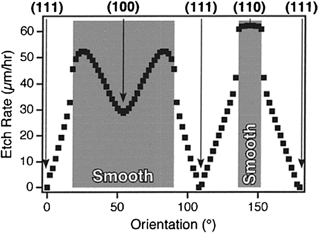
Fig. 2. Etch rate as a function of crystallographic orientation, determined using the microfabricated wagon-wheel. The transition between rough and smooth etch morphologies occurs at the same orientation as the etch rate discontinuities. Conditions: 70 C, 50% KOH. (From Ref.
obtained with hemispherical samples [19]. In addition, an atomistic approach using Monte Carlo simulation was used to explain the occurrence of protrusions on etched Si(1 0 0) and Si(1 1 0) surfaces and to study kinetic roughening [20]. Finally, the group developed two difffferent tools for continuum simulation of crystal shape evolution during etching.
上一篇: 单晶片工具上的栅极氧化物清洁
下一篇: 硅各向异性湿法刻蚀剖面演化的三维模拟