Metal oxide or metal nitride films are used as hard mask materials in the semiconductorlithography processes due to their excellent etch resistances against the plasma etchesChemical vapor deposition (CVD) or atomic layer deposition (ALD) techniques are usuallyused to deposit the metal containing materials on substrates or underlying films, which usesspecialized equipment and can lead to high cost-of-ownership and low throughput.The present paper describes formation and functional properties of novel metal oxidehard masks by simple solution spin coating process. These stable metal oxide formulationscontaining significant amount of Ti, W, Hf, Zr and Al possess good etch selectivity andtherefore good pattern transfer capability. The metal oxide films can be removed bycommonly used wet chemicals in the fab environment such as TMAH developer, solvents orother oxidizing agents.
The hard mask material absorbs DUV wavelengths and hence can be used as a spin-oninorganic or hybrid antireflective coating to control substrate reflectivity. Some metal hardmasks are also developed for via or trench filling applications for electronic devices as highK materials. The research demonstrated that these metal oxide hard masks are compatiblewith litho track and etch processing without concern of metal contamination. They cantherefore be integrated as replacements of CVD or ALD metal, metal oxide, metal nitride orspin-on silicon-containing hard mask films in 193 nm or EUV processes. This paper discussescoating, optical, filling, etch and wet removal properties the spin-on metal oxide formulationsIn addition, a new potential application in self-aligned quadruple patterning cut process foradvanced technology nodes is also described.
1. Introduction
As the feature size is getting smaller andsmaller, hard masks play an important role inpattern transfer to the desired substrate in the ICmanufacturing processes.Organic and inorganictype hard masks are used. While most organic hardmasks such as carbon and siloxane type are solutionspin coated, inorganic type hard masks such asSiON and SiN are either chemical vapor deposited(CVD) or atomic layer deposited (ALD). One ofthedisadvantages of these techniques is the throughputand high cost due to dedicated equipment needed[1] In the case of rework process, Si-based hardmasks have to be either removed by plasma etch or to be treated with strong oxidizing chemistries suchas concentrated HSO4/HO mixture (Piranha) withpost-removal process to clean off the residues on theSuch issues are challengingwafer surface.problems for manufacturability as they reduce thethroughput and yield due to high defects (2,3]Future generation of lithography processes requirehard masks with higher resistance to plasma etchand materials that can be easily wet stripped afterpattern transfer process to prevent dry etch damageto the substrate underneath (4,5]. Previously wereported that AZR Spin-on metal hard mask(MHM) materials are useful for generating metaloxide containing underlayers (4-9]. The materials demonstrated good long term shelf life and pot-lifestability. The underlayer coating is strippable inchemical solutions after curing of the film to formmetal oxide. The specially designed underlayers canbe used to significantly improve photosensitivity ofEUV photoresist performance [8,10]. The metaloxide films have excellent dry etch resistance and/orgood gap fill performances so that they can be usedas a hard mask to replace silicon underlayers inprocesses, such as trilayer or image reversalprocesses(4,5].
The present work will demonstrate theproperty, dielectriccoatingquality,opticalconstants, bulk etch rate, wet strippability, andfilling performance of our newly developed metaoxide hard masks containing Ti, Zr, Hf, W or AlThe etch performance is unique for each metalunder fluorinated gas or oxygen gas conditions. Forexample, the etch resistance of ZrOx films isgenerally higher than that of SiOx reference or TiOxfilms under CF4 plasma. For the same type of metalwith similar chemical platforms, higher metalcontents usually give better etch resistance. There isa trade-off between dry etch resistance and wetremoval process. Although most metal oxide filmscan be wet etched by alkaline chemical stripperssuch as SC1 (HO:HO2:NH4OH), developer orsimply polar solvents, high etch resistant ZrOx filmscan only be removed by aqueous solution of dilutedHF or Piranha (concentrated HSO4/HO2). Thegood filling feature of spin-on MHM materials canbe employed to yield a reverse tone image of theoriginal resist generally called image reversal ortone reversal after plasma etching the original resistpatterns [11]. The filling capability of MHMmaterials can also be used in device manufacturing.
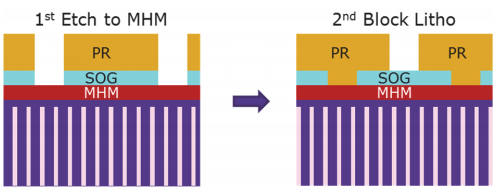
When the patterned substrate is part of an electronicdevice, the metal oxide film in the structure then canbe used for high K materials as gate dielectrics toreduce leakage current density [12]. To be used foradvanced patterning, the metal containing hardmasks will have to go through several lithographyand etch processes. Before introducing these newmaterials to the FAB, one needs to demonstrate thatthey do not induce any metal contamination in theprocess tools. We will report metal contaminationresults using both state-of-the-art litho tracks andplasma etchers for various metal oxide materialsusing TXRF (Total Reflection X-Ray Fluorescence)method. We will then present an example ofapplication of the metal oxide hard masks foradvanced patterning. Metal oxide hard masks canpotentially be used as etch stop layer in self aligned quadruple patterning(SAQP) cut last process foradvanced technology nodes below 7 nm since theyhave high dry etch and wet etch resistance during 1stetch and post-etch clean. (Figure 1). The etch stoplayer also serves as high etch selectivity hardmaskthat enables further pattern transfer to the substrate.

Figure 1
2. Experimental2.1. Material synthesis and formulation preparationDerivatives of metal alkoxide compoundswere synthesized at EMD Performance MaterialsCorp. In some cases, metal oxide nano particledispersions were used. Spin-on MHM formulationsdenoted as AZR EXP MHM samples in the resultsand discussion section were prepared by mixingappropriate amount of metal compounds andadditives in commonly used resist solvents such aspropyleneglycolethermonomethylacetate(PGMEA) or propyleneglycol monomethyl ether(PGME) or mixtures of PGMEA/PGME. AqueousMHM were also formulated where the metalderivative is readily soluble in water. The finalsolutions were filtered through a micro filter with apore size of 0.lum.
上一篇: 预氧化处理的影响
下一篇: GaAs 和GaN 的湿热氧化