Abstract
Nanoimprint lithography (NIL) is an emerging micro/nano-patterning technique, which is a high-resolution, high-throughput and yet simple fabrication process. According to International Technology Roadmap for Semiconductor (ITRS), NIL has emerged as the next generation lithography candidate for the 22 nm and 16 nm technological nodes. In this paper, we present an overview of nanoimprint lithography. The classfification, research focus, critical issues, and the future of nanoimprint lithography are intensively elaborated. A pattern as small as 2.4 nm has been demonstrated. Full-wafer nanoimprint lithography has been completed on a 12-inch wafer. Recently, 12.5 nm pattern resolution through soft molecular scale nanoimprint lithography has been achieved by EV Group, a leading nanoimprint lithography technology supplier.
Introduction
Nanofabrication, as one of the key domains of nanotechnology, has received intensive attention in the scientifific community. There are three approaches to nanofabrication: top-down, bottom-up and their hybrid approach. Top-down approach is referred to fabrication of smaller devices by using larger ones to direct their assembly, which has been developed based on the conventional IC fabrication process. Bottom-up process is to apply smaller components into more complex assemblies. More importantly, combined top-down with bottom-up is usually applied in nanofabrication. Nanoimprint lithography (NIL), invented by Stephen Chou et al., has been regarded as a possible alternative to optical lithography due to its low cost, high throughput and high resolution [1-8]. Since its invention, lots of research has been conducted in order to further develop NIL as a technology. To date, thermal embossing, laser-assisted, step and flflash and UV nanoimprint lithography have been incorporated into the fifield ofNIL. Since 2003, nanoimprint lithography has been accepted by International Technology Roadmap for Semiconductor (ITRS) as the next generation lithography candidate, and now has been added to 22 nm and 16 nm nodes. The resolution of nanopattern by nanoimprint lithograophy could reach sub-5 nm [9]. In this paper, we will elucidate fundamental theory and discuss some critical issues in nanoimprint lithography. Important research achievements are also presented in this review paper.
Classifification of nanoimprint lithography
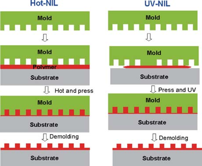
A schematic of the process of nanoimprint lithography is shown in Fig. 1. First, the substrate is coated with the polymer layer or functional layer, and the mold is pressed onto the polymer layer. After curing the polymer, the imprint mold is released from the layer. As a result, micro/nano patterns are transferred onto the layer. Usually, the patterns on the layer are etched by reactive ion etching process.

Fig. 1 Schematic illustrations for hot embossing and UVnanoimprint lithography.
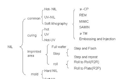
The main nanoimprint lithography technology is based on hot embossing lithography, UV-lithography and soft lithography. Depends on the kind of mold used, hard nanoimprint lithography and soft nanoimprint lithography are defifined accordingly. SiO2, Ni, Si, Si3N4, SiC molds are usually used for hard naonimprint lithography. Polymer materials, such as PDMS, PMMA, PUA, PVA, PVC, PTFE, ETFE, are main the components for the fabrication of soft molds. Depends on the curing approach to the spin-coated polymer, we have the difffferentiation into hot embossing lithography, UV nanoimprint lithography and hot-UV naoimprint lithography. Based on the imprinted area, the full-wafer nanoimprint lithography and step-and-repeat nanoimprint lithography are defifined. Roll-to-roll nanoimprint lithography process is suitable for mass fabrication, and has application in the state-of-the-art flflexible nanodevices. The classifification of nanoimprint lithography is indicated in Fig. 2. The details of the process could be obtained from the relevant literature.

Fig. 2 Classifification of nanoimprint lithography
Research fifield of nanoimprint lithography
Nanoimprint lithography technology encompasses the integration of subject areas including electronic engineering, machine engineering, control engineering, materials, physics and chemistry. Research and development on novel methods, process controlling, fabrication of equipment, as well as devices and system is therefore becoming more and more important. The goal is to develop fabrication equipment and process, resulting in low cost, high effiffifficiency and superior quality of the product. In the development of nanoimprint lithography, the basic processes and applications are highlighted. The basic processes include mold fabrication, the functional materials (imprint resists and transferred layer), controlling and optimization of imprint process and the development of imprint machine. The application fifields of nanoimprint lithography are in electronic devices (high density memory), photoelectric devices (solar cells, light emitting diodes), optical components (polarizers, lasers, TFT-LCD, plasma sensors) and biological fifields (biochips and microflfluidic devices) [10- 17]. The whole framework of nanoimprint lithography is outlined and shown in Fig. 3.
上一篇: 砷化镓中光学电子的自旋扩散
下一篇: 高效无臭氧抗蚀剂剥离工艺