Abstract: A new photonic integration technique is presented, based on the use of an indium phosphide membraneon top ofa silicon chip. This can provide electronic chips (CMOS) with an added optical layer (IMOS) forresolving the communication bottleneck, A major advantage of InP is the possibility to integrate passive andactive components (SOAs, lasers) in a single membrane In this paper we describe progress achieved in both thepassive and active components. For the passive part of the circuit we succeeded to bring the propagation loss otour circuits close to the values obtained with silicon; we achieved propagation loss as low as 3.3 dB/cm throughoptimization of the lithography and the introduction of Co (fullerene) in an electro resist, Further we report thesmallest polarisation converter reported for membrane waveguides ( <10 um) with low-loss (< 1 dB from 1520-1550 nm), >95% polarisation conversion efficiency over the whole C-band and tolerant fabrication. We alsolemonstrate an InP-membrane wavelength demultiplexer with a loss of 2.8 dB, a crosstalk level of better than 18dB and a uniformity over the 8 channels of better than 1.2 dB. For the integration of active components we aretesting a twin guide integration scheme. We present our design based on optical and electrical simulations and thefabrication techniques.
Introduction: The IMOS platform is based on a high refractive index contrast InP membrane, which is optically verysimilar to a silicon membrane and suitable for the creation of high-density, low-power PICs. In the long term, we wantthe full functionality ofclassical InP-based PICs to be integrated in IMOS, using a set of standard building blocks. Thestrength of the IMOS concept resides in its inherent ability to integrate active and passive functions. We follow the samephilosophy as the Generic Integration approach for in classical InP-based PICs (1] as illustrated in figure 1. With alimited set of basic building blocks and a generic process we are able to make a great variety of A(pplication) S(pecific)P(hotonic) I(ntegrated) C(ircuits.

Also in IMOS we want to develop a Generic Integration Process in which active and passive components can be integrated.

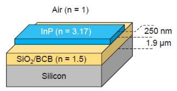
Figure 2 represents the typical dimensions and composition f an IMOS waveguide. InP (n = 3.17) is chosen as the highrefractive index wave-guiding material, because of its ability to integrate lattice-matched active and passive materials.The low-refractive index (n = 1.5) polymer Benzo-Cyclo-Butene (BCB) is used as an adhesive to bond the Inpmembrane to a Silicon wafer. The thickness of the InP membrane is chosen as 250-300 nm to obtaina strong light confinement, while a bonding layer thickness of 1.9 um enables to decouple the nP membrane from thehigh-refractive index silicon wafer both optically and thermally. The InP membrane can also contain an active layer foractive components.
上一篇: 硅碱性蚀刻中的绝对蚀刻速率
下一篇: InP硅集成的均匀性研究